I have built JLH´s simple 30W amp (mosfet version with 50W). It oscillates with a reactive load and I have a hard time tracing the problem, since I don´t understand how the first stage works.
JLH uses this first stage in virtually all older designs until he went LTP, so the 1969 10W class-A amp has it too.
I do not understand, how this stage works, it looks much different to all contemporary desings I know.
Lateron Geoff and AndrewT have modified this stage with a CCS, unfortunately without revealing the design criteria.
I´ve tried to contact both with no luck.
Can anybody describe what this stage does.
Thanks.
Member
Joined 2009
Paid Member
Oscillation - what frequency (roughly ?)
Very high frequency (MHz) is likely the FETs self-oscillation. Do you have an output zobel network, a 10R resistor in series with 100nF capacitor between output and ground ? The FETs may have other oscillation modes, do you have gate stopper resistors ? With really fast FETs you might also need a zobel network (resistor in series with cap) between gate - drain
High frequency (100's KHz) is likely feedback loop instability. Can be caused by poor wiring or grounding but also lack of adequate frequency compensation for the feedback. JLH didn't use any in his 1969 Class A design, the slow output devices were enough. For your amplifier you need something else. A common approach is a small capacitor (100pF) between base-collector of the voltage amplifier transistor (VAS) but JLH used other techniques.
What is your 'reactive load'?
What active devices are you using?
What is the frequency of the oscillation, and the amplitude?
What quiescent are you using?
What are your compensation values, and where?
Can you show us a picture of both your schematic and your implementation?
Like Jonathon I am concerned that you are unwilling to examine the huge, expansive thread. It sounds to me that you want someone else to give you a quick fix without passing through the necessary learning curve that most of us undertake as our rite of passage..........
Hugh
I did not want to bust into the class-A thread. My problem has very little to do with it.
I learned however, that this is the JLH freak´s abode.
Concerning the rite of passage:
I am a teacher. If a student turns to me with a specific question on a new subject, and I hand him a 350+ pages book and tell him "your answer lies possibly somewhere in here" then this is not very encouraging. I did not ask somebody to provide an off-the-shelf fix for my problems, I will sort that out myself with luck, but I asked for help for a specific problem. If that is asked too much I´d have to renounce to ask for help.
Hi,
The input singleton is very simple to understand.
Try TinaTi simulator if your getting confused.
Death of Zen - A new Class-A power amp
Might help understand the input and feedback.
rgds, sreten.
The input singleton is very simple to understand.
Try TinaTi simulator if your getting confused.
Death of Zen - A new Class-A power amp
Might help understand the input and feedback.
rgds, sreten.
You're not likely to solve the problem without knowing a whole lot more than you already do. So, rather than read the 350 page book - an answer that I have always found incredibly obnoxious, btw - you might want to learn something by first answering the questions, since those will let others focus your attention.
Btw, 90% chance the problem is not in the front end... fwiw.
_-_-bear
Btw, 90% chance the problem is not in the front end... fwiw.
_-_-bear
Helmut,
As a teacher, I am surprised that you asked questions without the basic observations.
However, to come back to the questions:
What is your 'reactive load'?
What active devices are you using?
What is the frequency of the oscillation, and the amplitude?
What quiescent are you using?
What are your compensation values, and where?
Can you show us a picture of both your schematic and your implementation?
And to add, measure all the base/emitter voltages on all active devices. Anything different to 0.6-0.7 volts points generally pinpoints issues. Most of the problems surround the active devices.........
Hugh
Folks,
to first answer the questions you implied, then those you asked.
I agree.
I bought Bob Cordell´s book and wanted to go through my design in analogy to the way he describes. Unfortunately I stumbled over the first stage, which I now know at least the name of. Reading an endless thread on matters that are 98% nothing to do with this subject did not promise anything. The class-A business is about an entirely different subject and has with the simple 30W amp just the first stage in common and the author.
Absolutely. Please appreciate that I never planned to have my problems with this amp solved by others, taking a shortcut. This was never my question. But now you offer specific help and I gladly accept.
Please appreciate that I just asked one question regarding the first stage. That is not related to any observations.
> What is your 'reactive load'?
As specified by JLH this is 8Ohm/2µF. The amp was stable BTW with 0.1µF
>What active devices are you using?
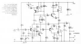
Compound transistor/ lateral mosfet pair, these days allegedly called "sziklai pair". Pls. see schematic for more.
>What is the frequency of the oscillation, and the amplitude?
Powering the amp up with a variac and a bulb current limiter I noticed HF fuzz riding on top of the sinewave. From memory, this was not as high frequent as I expected (MHz), rather below 100 kHz on a 1kHz wave.
>What quiescent are you using?
I adjusted the quiescent current to 100mA as recommended by JLH for lateral mosfets, but then forgot to plug the bulb limiter in again and on the next power-up the output devices blew. I now wait for new ones.
>What are your compensation values, and where?
Typical JLH compensation directly on the input device. JLH claimed total stabilty with 47pF and perfect square wave behavior.
>Can you show us a picture of both your schematic and your implementation?
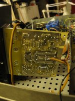
attached. I used the 2S type transistors for the preamp stages and the 2N types for the output pair. In case you wonder about the funny transistor sockets. These are my "universal" footprints that let me accomodate any transistor during evaluation.
>And to add, measure all the base/emitter voltages on all active devices.
Currently not possible. Waiting for new output devices.
The amp ran for hours with an actual speaker, just failed the reactive test and thus is not unconditionally stable and reliable.
Reading in Bob´s Book I immediately detected a few possible layout shortcomings like insufficient local decoupling.
-helmut
to first answer the questions you implied, then those you asked.
You're not likely to solve the problem without knowing a whole lot more than you already do.
I agree.
So, rather than read the 350 page book
I bought Bob Cordell´s book and wanted to go through my design in analogy to the way he describes. Unfortunately I stumbled over the first stage, which I now know at least the name of. Reading an endless thread on matters that are 98% nothing to do with this subject did not promise anything. The class-A business is about an entirely different subject and has with the simple 30W amp just the first stage in common and the author.
you might want to learn something by first answering the questions
Absolutely. Please appreciate that I never planned to have my problems with this amp solved by others, taking a shortcut. This was never my question. But now you offer specific help and I gladly accept.
AKSA said:I am surprised that you asked questions without the basic observations.
Please appreciate that I just asked one question regarding the first stage. That is not related to any observations.
> What is your 'reactive load'?
As specified by JLH this is 8Ohm/2µF. The amp was stable BTW with 0.1µF
>What active devices are you using?
Compound transistor/ lateral mosfet pair, these days allegedly called "sziklai pair". Pls. see schematic for more.
>What is the frequency of the oscillation, and the amplitude?
Powering the amp up with a variac and a bulb current limiter I noticed HF fuzz riding on top of the sinewave. From memory, this was not as high frequent as I expected (MHz), rather below 100 kHz on a 1kHz wave.
>What quiescent are you using?
I adjusted the quiescent current to 100mA as recommended by JLH for lateral mosfets, but then forgot to plug the bulb limiter in again and on the next power-up the output devices blew. I now wait for new ones.
>What are your compensation values, and where?
Typical JLH compensation directly on the input device. JLH claimed total stabilty with 47pF and perfect square wave behavior.
>Can you show us a picture of both your schematic and your implementation?
attached. I used the 2S type transistors for the preamp stages and the 2N types for the output pair. In case you wonder about the funny transistor sockets. These are my "universal" footprints that let me accomodate any transistor during evaluation.
>And to add, measure all the base/emitter voltages on all active devices.
Currently not possible. Waiting for new output devices.
The amp ran for hours with an actual speaker, just failed the reactive test and thus is not unconditionally stable and reliable.
Reading in Bob´s Book I immediately detected a few possible layout shortcomings like insufficient local decoupling.
-helmut
Attachments
Last edited:
WRT the the devices, I expect the question is not so much what is the topology (circuit) but the actual devices used. This pertains to their ft or "speed" as compared with the original devices. Faster, newer devices may require a slightly different compensation scheme.
The other thing that was requested is a picture(s) of your actual amp or amp modules as they are now. With these amplifiers, stability DOES depend on layout and "wire dress".
One fellow in another thread here complained about his amp not being stable, even though almost everyone else's has been stable. After much discussion in the thread and without the benefit of images of the actual amp it finally became clear that the builder had it in his head to neatly "bundle" the wires going to the output devices. Hopefully, it is clear to you why this is a terrifically poor idea?
So, with images of the actual build "bad practices" may be spotted.
Btw, buy yourself a copy of Art Of Electronics (first Edition is fine for analog stuff, btw). It is a superior reference and source of circuit insights. Cordell's book is an advanced text.
Wise words, Bear. I've had so much trouble reworking repairs and DIY builds made with cheap bogus or generic knock-off semiconductors. It seems people are happy to overspend on gilt-edged electrolytics but not much attention is paid to the active components.
It seems though, that this amplifier works OK with a speaker but not with a "reactive load". Perhaps that load is the kind that any amplifier would have problems with. A little more detail would help understanding whether the problem is as bad as it seems.
Otherwise, when you look at all those long obsolete parts specified by JLH, even in this later Mosfet version, there will be compromises and probably reduced stability when virtually every semiconductor is substituted. One or two substitutions may be fine but the sum all changes is likely a cumulative problem that needs a systematic solution.
Ian, he says in the above post that he has some "fuzz" riding the sinewave when run into a lightbulb (?) as a load. This says parasitic oscillation (of course). So, the reactive load merely send the amp off into oscillatory heaven.
Until we hear back from the OP, not much more can be said or done.
_-_-
Until we hear back from the OP, not much more can be said or done.
_-_-
OK.
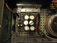
I made pictures from the top and bottom. I believed this can be seen from the printouts in the PDF and did not think of a photograph. The PDF has several pages.
The output devices are directly mounted to the pcb and transfer heat (hopefully well) to a heatsink via a 5mm aluminium bracket. Pls. see photo.
These are, as printed in the PDF, 2SK1056/2SJ160, obtained from reichelt.de. I have heared about fake units, but I have no method of verifiying their validity. They sure don´t have "renesas" printed all over them, but that alone would not have arisen my suspicion. They were the only company that seemed to stock them. Note that on the website they only show a generic picture
The mosfets used are successors of the obsoleted original types and may have different behavior.
None of the semiconductors uses are available today, only claimed replacement types made out of unobtainium.
In a later article JLH said, that his choice of low power transistors was mainly down to the fact that he had stacks of them at home.
In a similar amp he then recommended more generally "low power transistor, 100mW" or "medium power transistor 600mW" or similar.
I took the ones mentioned earlier for voltage capability and power (2N5551), resp. 2SA970 for low noise. (Incidentally, Geoff Moss used the latter in this later 10 watter...).
But in sum they may behave not as expected and require a thourough analysis.
The test load is a common wirewound power resistor with a 2µF film cap in parallel.
JLH always uses this reactive test load to proof stability on square wave inputs. My rendering of the amp may have just worked with the speaker attached, however it may have exhibited ringing or similar.
With lightbulb I mean "the poor man´s current limiter", a 100W bulb in series with the mains.
Even with zero input signal the bulb would light up considerably more than without the cap, indicating there was some excessive current consumption. This was dramatically increasing as soon as the output was excited.
Let me know it here is any more pics needed.
-helmut
Attachments
- Status
- This old topic is closed. If you want to reopen this topic, contact a moderator using the "Report Post" button.
- Home
- Amplifiers
- Solid State
- JLH 1969 first amplification stage, need explanation