In 1980 I built the Maplin 225WRMS disco amplifier with pair of 2N3055 and pair MJ2955.2N3055 = Slow:
They are fast enough for a near perfect 50KHz square wave without any overshoot and a bandwidth beyond 200KHz. Their Ft(=0.8MHz to 4MHz) prevents high frequentie oscilation. I consider it useless to use faster ouput transistors if that mean installing of an compensation cap which I now do not need. This design is inherent stable.
2N3055 = bad gain linearity:
Well considering that this design uses the 2N3055 at 1.2A Iq thus so only at a 0.1 to 2.2A current swing, the devices are used in their lineair regeon (well according to D. Self in his book). Add to that that I discoved I do not need mor then 0.5A current swing for high SPL levels I considerd it as not so important
2N3055 = not robust
Well they are use at an Iq of 1/7th of the rating and a power dissipation 1/10th of their rating. I do not have to expect any failers.
Seems to me that no argument against the 2N3055 can be made other than the most important:
Subjective Experience.
The amp got hammered to within an inch of its life at ever gig I did.
It was still going strong 5 years later when I sold up the disco.
Only ever had one complaint about the sound, too flipping loud !
High fidelity class A audio for low power personal use though, is a different animal. By reputation, I think most listeners will be expecting to hear something close to the best possible sound quality from this very popular little JLH amp, whatever types of semis were used in the construction.
By reputation, I think most listeners will be expecting to hear something close to the best possible sound quality from this very popular little JLH amp, whatever types of semis were used in the construction.
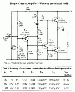
I agree, and I would like to add that it is desirable to use speaker systems with an impedance of 8 ohms and a sensitivity of at least 91dB in the load. It is also necessary to add RC chains to limit the frequency spectrum of the input signal - this will improve the transient response.
Use instances with maximum Hfe (at a current of 1-1.5a).but given the huge quantity of my original Motorola and RCA 2N3773 even if they are obsolete, I will try them ...
Last edited:
Re: #8463
Limiting the signal bandwidth is seldom discussed here. Perhaps that's because of a common notion that supersonic bandwidth is somehow better. So, what characteristics or design would you suggest for this type of limiting filter?
the input RC filter limits at a frequency of 0.72 MHz, which is less than the frequency of unity gain per octave, and RC in the NFB circuit approximates the gain reduction to the unity gain frequency to a drop of 19dB per decade.
Attachments
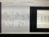
I focus on the transient response, see attachment.Thanks for the suggested details. Where there are problems with local solar power, industrial power systems and radio transmitters etc, I expect RFI and EMI would be reduced significantly too.
Attachments
Yet I run into "design engineers" who think that, as long as the PCB matches the schematic, nothing can possibly be wrong with the layout and routing. What hope do poor amateurs have without some rules of thumb ?I'm not sure whether you're agreeing or not. Of course I'm not suggesting that a badly designed board is going to work.
For the record, I worked with boards that simultaneously carried GHz RF, microprocessors and DSPs, analogue audio, and switch-mode power regulators. Then I had to get them through EMC testing. So I'm well aware of parasitic coupling")
To illustrate benefit of input signal bandwidth limiting, here is measurement taken on simple diamond buffer with CFP output stage and measured power bandwidth of 1.6 MHz (220 ns rise time). This is unity gain buffer with no GNFB.
As this is prototype assembled on the breadboard, there are enough parasitic inductances from long wires to introduce solid resonant gain peaks at very high frequencies.
Square wave input signal with bandwidth above 20 MHz (15 ns rise time) will trigger all those parasitic and effect is visible as ringing.

Now, if we limit input signal to 200 ns rise time, amplifier output signal is clean, with just slightly increased rise time, while no changes were made on the amplifier circuit. Input RC filter does just that, limits input signal rise time, as was done using controls on signal generator.

Usual audio signal can’t have such fast rise, but if someone is fan of NOS DAC with unfiltered output (leaving filtering to rest of audio chain), it would be good to consider eventual consequences.
As this is prototype assembled on the breadboard, there are enough parasitic inductances from long wires to introduce solid resonant gain peaks at very high frequencies.
Square wave input signal with bandwidth above 20 MHz (15 ns rise time) will trigger all those parasitic and effect is visible as ringing.
Now, if we limit input signal to 200 ns rise time, amplifier output signal is clean, with just slightly increased rise time, while no changes were made on the amplifier circuit. Input RC filter does just that, limits input signal rise time, as was done using controls on signal generator.
Usual audio signal can’t have such fast rise, but if someone is fan of NOS DAC with unfiltered output (leaving filtering to rest of audio chain), it would be good to consider eventual consequences.
Thanks Hennady! I will try! Today my circuit looks like this:I focus on the transient response, see attachment.
Monoblock amplifier:
PDF Ciruit:
https://drive.google.com/drive/folders/1hqNqf1LpdyNb26nMPSwo5KOk3z-7M26V
Test video amplifier:
https://www.youtube.com/playlist?list=PLceAdLTPocSHFkuiKAzEND4Blkb3-oGuQ
Modeled JLH again. The basic parameters are somewhat worse than in the amplifier that I previously set. But I made an attempt to improve the standard JLH, and the attempt was successful. The added D1 R2 circuit in the Q4 base circuit halved distortion and increased the maximum undistorted output voltage. You can add it to your ready-made amplifiers. 👍
Attachments
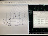
You're right. I haven't used it for a long time. Here is the original scheme. And in this case, the presence of the D1 R9 circuit allows you to correct TND by changing the resistance of the load circuit Q1 for positive and negative half-waves.
Attachments
Thanks Hennady! I will try! Today my circuit looks like this:
Monoblock amplifier:
View attachment 1098315
PDF Ciruit:
https://drive.google.com/drive/folders/1hqNqf1LpdyNb26nMPSwo5KOk3z-7M26V
Test video amplifier:
https://www.youtube.com/playlist?list=PLceAdLTPocSHFkuiKAzEND4Blkb3-oGuQ
I note the use of high Ft output transistors 2SC5200 and discussions of low pass filtering at the non-inverting input to avoid intrusion of environmental hf signals from inter-modulating with audio signals.
It is easy to overlook that an inverting input exists at the emitter of Q4, with potential risks that environmental signals can be induced into lengths of cable or coils of wire such as loudspeaker coils and crossover inductors. Also loudspeakers are alternatively back and forth motors/generators.
The JLH design has no internal capacitors limiting the frequency range of the voltage stage. This needs to be reduced to less than unity = 1 before phase reversal at 180 degrees.
Due to 2N3055 having lower operating frequency than the other transistors in the circuit the output devices set an inbuilt dominant lag. JLH claimed this made the circuit unconditionally stable.
Transistors like 2N3055 where the transition frequency is low can be described as slow in terms of switching times and having roughly a tenth of 2SC5200 the gain bandwidth product and longer switching times.
In a constant current Class A system there is zero switching to be done and 2SC5200 has no practical advantage. The disadvantage these have is excessive response out into the 30 MHz frequency range where modern electronic devices generate signals which have potential back door entry.
To keep dust or leaves from blowing into the house who would think of having a door 30 feet wide where one 3 feet wide would do.
To reduce the transition frequency with 2SC5200 to the same level as 2N3055 to attain the same stability margin, a common DIY approach is to add a capacitor in parallel with R3. The impedance of capacitors reduces with increasing frequency so there is a bypassing effect with R3 - this strategy can impose a risk.
A better approach would to create step response network by an RC network in parallel with R3 such that loop gain falls below unity by a safe margin leveling off somewhere below the associated frequency point.
The closed loop gain of this amplifier is quite low. If the line stage to drive this is based around an IC op.amp for the lowest THD the closed loop gain of this should be of the order of no more that 2 according to articles by JLH on pre-amplifier design.
In combination the total amplification is low if the preamplifier as padding resistor networks for input sources so the signal levels are equal when selected.
There is some potential in using devices like 2SC5200 to allow an increase in the closed loop gain of this circuit. The increase in gain will result in a reduction in frequency response.
"In a constant current Class A system there is zero switching to be done and 2SC5200 has no practical advantage. The disadvantage these have is excessive response out into the 30 MHz frequency range where modern electronic devices generate signals which have potential back door entry."
That does appear to be so, at least in my experience and I think John Ellis may also have raised this point here in the past. I also think that many people get stuck on linear, class AB design principles which have been foremost in most audio educational discussions and electronic design papers for so long. Even class D still hasn't entered the consciousness of some folk who have been listening to it, perhaps unwittingly, for some years too. Others probably think of audio amplifiers as just a mesh of wires and components with an input and output and so their simulations will only treat that much. After all, modelling audio circuits is complex enough without trying to predict EMI and RFI susceptibility. Anyway, I was interested in this aspect of the amp. some time ago and I tested a few JLH kits, one being already designed for T03P(L) style output transistors like 2SC5200, so it received quite a lot of abuse.
I just assumed fakes would be not be much of a problem in a design suited to low Ft semis. Those supplied may have actually been genuine spec. because there are several manufacturers offering their versions of 2SC5200/2SA1943 very cheaply and it's difficult to guess what you will actually receive when generic images are simply copied from one competing seller site to another. What happened with 2 examples, was that I did hear some detected audio noise and see some significant RFI/EMI on the oscilloscope. Then I simply substituted MJL21193 which reduced the problem considerably when using loudspeakers but I'm not sure that will help those who use sensitive headphones with the JLH.
The MJL series power transistors will probably be too expensive for a lot of people and there are other suitable, cheaper, low Ft transistors available in plastic flatpack forms which will fit in the same location. At the lowest level, I tried out STMicro TIP3055. No surprise, it sounded much like their obsolete 2N3055 but at least it was silent with regard to RFI/EMI. Next, I tried KTD1047. There are also Chinese producers of this D1047 type and its difficult to know the source or quality so I avoid that generic type. Apart from the package, these seemed similar to C5200 so they may be closer in quality than the specs suggest....YMMV
Last edited:

Hi Ian,
I endorse your message to take care with choosing transistors.
I looked at ST Micro's and ON Semiconductor's datasheets for TIP3055 which come in more modern TO-247 plastic cases and consider these are wise choices.
These parts are also sold over the counter in SOT-93 packaging by Jaycar Electronics. The latter could be adequate for low power outputs but not have as long a service life as for those two brands.
For premium quality parts one would have to buy from a warehouse with additional costs for picking, packing, and postage.
For myself, I would consider MJL3281 parts instead of TIP 3055 as the former have a minimal collector -emitter saturation voltage at the operating current levels required for this design and lower voltage supply rails can be used.
Also the power rating of MJL parts is double TIP 3055 and the hFE graphed against current is more linear.
The Gain Bandwidth Product is also ten times better. Thus the same frequency range as for TIP3055 can be achieved by increasing the closed loop gain of the circuit to obviate the need for a line stage. That would and allow a direct input through an input selector switch and volume control.
There is also a question of matching current gain for the best THD figure as stated in the original 1969 article.
For NPN/PNP MJL3281/MJL 1302 complementary pairs gain matching is within 10% from 50m.a. to 5A. (this comes from the On Semiconductor datasheet)
For transistors of the same type MJL3281A gain match has to be much less than 10 % within the above stated range, as the distributions in the N and P silicon doping layers is identical.
The distributions between these and those in MJL1302 are different.
The carriers in N type silicon doped with Aluminium are electrons. These are more mobile than holes (absences of electrons) in P type silicon doped by Phosphorus.
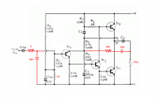
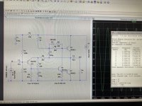
Hey all, my JLH is showing some initial signs of life but with some strange behaviours and I need some ideas
It is pretty much following the JLH69 schematics with:
Transistors: BC559, BD139 and BD249C
Power is right now an 18v / 6A laptop SMPS and my speakers are 8Ω
I have hooked everything up, set the Vx to half (9v) and started to test out with some music source.
If you look at the attached JLH circuit part names I have an 100Ω for R1 and 1K pot for R2.
I only manage to get clean sound when R2 is turned all the way to one end and while turning it towards the other direction the sound gets distorted pretty badly.
At the same time whats really weird is:
Any ideas or suggestions would be much appreciated!
It is pretty much following the JLH69 schematics with:
Transistors: BC559, BD139 and BD249C
Power is right now an 18v / 6A laptop SMPS and my speakers are 8Ω
I have hooked everything up, set the Vx to half (9v) and started to test out with some music source.
If you look at the attached JLH circuit part names I have an 100Ω for R1 and 1K pot for R2.
I only manage to get clean sound when R2 is turned all the way to one end and while turning it towards the other direction the sound gets distorted pretty badly.
At the same time whats really weird is:
- with R2 all the way with the clean sound TR3 (BD139) and R1 (100Ω) get really hot but the two Transistors attached to the heatsink stay cold.
- with R2 all the way to the other end TR3 and R1 are not as hot and the heatsink transistors are still cold.
Any ideas or suggestions would be much appreciated!
Attachments
- Home
- Amplifiers
- Solid State
- JLH 10 Watt class A amplifier