Most of that is the current through C1, the bootstrap capacitor. Plus a couple of mA through R3.
Ah. I thought I'd checked that. You are, of course, correct and thank you.
Here is the little teaser I promised classAchap... its a bit off topic but it was interesting and came about through questions asked on this amp earlier in the week.
The file is a simple (as simple as it gets) complementary output stage. Single rail of 10 volts with an AC coupled load to ground. The input is a sinewave biased "or sat upon" 5 volts DC so that we get max output swing. The output shows the classic class B crossover distortion.
So far so good. If you look at the voltage across the load and the current in the load you will see they are as expected, and in phase. Its educational to now look at the current in the output cap C1 and you can see how its 90 degrees out of phase with the voltage, the current in a capacitor leading the voltage by anything approaching up to 90 degrees if the cap is big enough in relation to the series load resistor.
If we now look at the current in the load which rises to around +160 milliamps on positive half cycles and -160 milliamps on the negative half cycles and then superimpose on that the current in R1 (which is in series with the supply) we see something that isn't very intuitive
If the input signal is now changed to a single half cycle (as shown... it takes a few seconds to run as a sim due to it being in the "dead crossover zone) the circuit "appears" to draw no current from the rail. I'll leave that one with you
Attachments
Hello good experts!
I'm in need of some assistance. Just finished building a JLH (from siliconray).
Bias is set to 1.2A. Voltage is about 26V.
The problem is: It works fine on a couple of 4ohm speakers. (Some hum I haven't tried removing yet). But once I connect a pair of 6 ohm fulltone speakers (elements from markaudio), the amp goes haywire. DC on the outputs rises to more than 2V, and the speaker protection kicks in.. With only one of the speakers connected, the DC sits at about 1.7V.
Anyone have an idea of what might be wrong?
Last edited:
Hi zajin. That IS odd. Can you clarify something please? When you talk about DC at the output what exactly do you mean? Is your amp the later 1996 split rail version with NO output capacitor? And not quite sure what you mean "with one of the speakers connected". Is that one of a stereo pair? I.e. only one channel? I am just a bit confused by that.
The first thing I'd do is check the DC resistance of the speakers. Might sound obvious but the speaker may be "shorting out".
I guess you have others amps. Have you tried the different speakers on another amp'?
Increasing the load from 4 Ohms to 6 ohms should not make the amp' go crazy.
Best of luck,
Jonathan
Thanks for answering. I see I was a bit unclear in my explanation.
Yes, it's the 1996 (or 2005, this one: JLH 2005 Class A Amplifier Kit - Boards | Kits | Components | Modules | Tools)
I measure DC voltage on the speaker terminals. With no speaker connected it's about 20mv, same with the 4ohm speakers. When connecting one of the 6ohms, the voltage rises instantly to -1.7 on that channel.
Both speaker-pairs works perfectly with an older marantz integrated, no problems there..
Ahh.. found the problem. It was actually the speaker cables I used for the 6ohms.. (home made braided cables made from cat-5, never had a problem with them before). For some reason they sort of behaved like a capacitor and this amp did not like that. Changed to regular cables and all is well!
Thanks for taking the time to answer!
Now for getting rid of hum, will probably try to double or triple capacitance in PS.
Thanks for taking the time to answer!
Now for getting rid of hum, will probably try to double or triple capacitance in PS.
Ahh.. found the problem. It was actually the speaker cables I used for the 6ohms.. (home made braided cables made from cat-5, never had a problem with them before). For some reason they sort of behaved like a capacitor and this amp did not like that. Changed to regular cables and all is well!.
How did you work out it was the capacitance of the cables?
A Pi type Thiele Network between the amp PCB and the output terminals will make the amp immune to cable capacitance variations.
I never build an amp without this Pi Filter/load.
The output Zobel must be returned to the PCB Power Ground as close to the Output devices as possible.
I never build an amp without this Pi Filter/load.
The output Zobel must be returned to the PCB Power Ground as close to the Output devices as possible.
I am experimenting with a version of Geoff Moss's optimised JLH and have designed a small PCB for it (fig. 2 here: The Class-A Amplifier Site - JLH Class-A Update)
The amp seems stable enough and behaves more or less as expected, but I have a rather large DC offset on the output (trimmable from app. 10V to app 6,5V on both channels). Does anyone know what could be the source of this?
I have obviously checked the layout and component placement and I see no obvious blunders (which is not to say that there aren't any, obviously).
However, I have also looked at the schematic and realised that the trimpot VR1 has changed from 2k to 200R between the two versions of the schematic in the article (compare fig. 1 and fig. 2). Could this be the problem? It seems to tally with being able to trim the offset, but not having enough range to zero it?
/U.
The amp seems stable enough and behaves more or less as expected, but I have a rather large DC offset on the output (trimmable from app. 10V to app 6,5V on both channels). Does anyone know what could be the source of this?
I have obviously checked the layout and component placement and I see no obvious blunders (which is not to say that there aren't any, obviously
). However, I have also looked at the schematic and realised that the trimpot VR1 has changed from 2k to 200R between the two versions of the schematic in the article (compare fig. 1 and fig. 2). Could this be the problem? It seems to tally with being able to trim the offset, but not having enough range to zero it?
/U.
Member
Joined 2009
Paid Member
I'm planning on trialing a choke input power supply to drop the hum/hash radiated by power supply.
I didn't have enough voltage off the trafo secondaries for that (as you know, switching from cap input to choke input means you lose around a 1/3 of the rail voltage) but I would've done what you suggest had it been possible. What I've done with mine - made a C-L-C supply.
Last edited:
Member
Joined 2009
Paid Member
However, I have also looked at the schematic and realised that the trimpot VR1 has changed from 2k to 200R between the two versions of the schematic in the article (compare fig. 1 and fig. 2). Could this be the problem? It seems to tally with being able to trim the offset, but not having enough range to zero it?
/U.
I believe the input stage needs more current in the 'final' version than in the 'penultimate' version so you do need the 200R rather than 2k in order to get more current flowing to the emitter of the input transistor. The way I see it, this higher current is used to compensate for the removal of the shunt feedback cap. Without this cap the feedback shunt resistor allows for a dc flow of current to ground, starving the input transistor of current. This forces the input transistor to source the missing current through the series feedback resistor (from the output) thus developing a voltage across the feedback series resistor. This voltage shifts the dc offset away from where you want it. By providing sufficient current to the input device emitter through the current source you can compensate for this and reduce or eliminate the dc current flow through the series feedback resistor so that the dc offset moves back to zero.
What you could do is to parallel the trim pot you have with a smaller valued fixed resistor til you get the dc offset in the right range - then the trim pot will give you a 'fine adjust'.
Plus - you could put a cap into the feedback shunt circuit (like the Penultimate circuit) to get it up and running. That would allow you to ensure everything else is to your satisfaction and give you a reference 'sound' to compare with if and when you take the cap back out.
Last edited:
Thanks for the reply. If by "feedback shunt capacitor" you mean C4, then it is already there. I deliberately left it in because it says in the article that taking it out may cause hum issues. So does this mean you think I should in fact replace the VR1 trimmer with 2k?
However, since you also mention the link between the current in the Q5/Q6 CCS and the offset, what is a "normal" value for this current (measured, I assume, as the voltage across R11?)
/U.
However, since you also mention the link between the current in the Q5/Q6 CCS and the offset, what is a "normal" value for this current (measured, I assume, as the voltage across R11?)
/U.
Last edited:
Member
Joined 2009
Paid Member
I don't believe R11 is carrying the same current that flows through the input transistor; R11 provides bias for Q5, which in turn measures the current through VR1 and controls the base voltage on Q6 in order to produce a constant current through Q6 - hence CCS. To measure the current out of the CCS you can get a reasonable estimate if you measure the resistance of VR1 (when powered off) and then measure the voltage across VR1. I haven't simulated (or built) this exact version but if I remember correctly, the input transistor is expecting under 1mA of dc current (closer to 500 uA). I'll check it with a sim - wait a minute....
Last edited:
Thanks for the reply. If by "feedback shunt capacitor" you mean C4, then it is already there. I deliberately left it in because it says in the article that taking it out may cause hum issues. So does this mean you think I should in fact replace the VR1 trimmer with 2k?
/U.
Yes! You need the higher 2k value in this case.
Tim
Member
Joined 2009
Paid Member
Quick simulation - current through input transistor is low, about 1/3 mA.
Another thing to bear in mind is that dc offset also depends a bit on the temperature. There is also a bit of dependency on the current through Q3 since it will draw a base current from the input transistor.
You'll want to use the higher valued trimmer for VR1 when C4 is installed. In my simulation VR1 needed to be set at around 1.2k and VR2 at 10R.
Also from the simulation, R11 has around 16V across it.
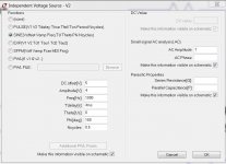
Attachments
Last edited:
Hi all
MJL3821A transistors can be used in the JLH amplifier (at least in my version) as long as you add a small compensation capacitor across the feedback resistor. The value needed is somewhere around 33pF as I recall. The additional gain (min. 75) will reduce the distortion compared to MJ15003/MJ21194.
I wondered if the reported "hum" reported with MJ21194's is because the samples had a higher gain than MJ15003. The MJ21194 transistors have a high gain hold-up so may well draw more current. I suspect the amps in the power supply increased to cause the hum, but also I presume the Iq was adjusted correctly for each type.
On the other hand hum, usually caused by heavy currents drawn from the PSU, may also indicate oscillation...
Cheers
Hi all
And another point regarding the JLH. If the input current is only about 250 microamps the emitter resistor (the one on the ground side of the feedback network) should not be greater than 100 ohms IMHO. I'm using a rule of thumb that says the external resistance ought to be no greater than the internal Re. If the 270 ohms is reduced to 100 and the feedback resistor to 1.2k (maybe 1W too) then the distortion should be halved ...
Cheers
- Home
- Amplifiers
- Solid State
- JLH 10 Watt class A amplifier