Counterculture, thank you! It's added to my reading list, I am sure to cover a lot of things I am missing. As for the FETs I am using here, they are 2N5638, they belong to the "switches and choppers" class, same as J111, J112, J113 etc. Their ON resistance is at around 10-20 Ohm.J111 & J112 are ideally suited to FET switching. If the source is treated as the input then it should be strapped to the gate using ~22k to ensure that Vgs remains @ 0V in the presence of an input signal. These FETs are apparently symmetrical.
Rather than try to reiterate the entire section from the book, I would suggest reading pages 408-421 of Small Signal Audio Design by Douglas Self which contain a comprehensive treatment of this subject.
On the circuit I have the Drain facing the signal input and Source facing the signal output. But yes, these FETs are symmetrical.
Now I get it!Mooly said:You must drive the FET's via a resistor. The diode leaves the gate floating which is no good. Make sure that -14 volts is within the G-S rating of your chosen FET.
My misunderstanding here was that from 0V and upwards(+) the JFET's resistance would not change, hence my proposal of using a diode.
So, if I get it right, when the JFET is ON (Vc=0V) the resistor will be conducting the necessary offset to the gate.
When the JFET is OFF (Vc=-13) there will be some of the gate's negative voltage present... Won't I be needing some caps after each JFET for not having DC injected to the signal?
Here is the circuit with the 22k resistors added:
Attachments
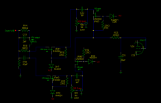
22k is too low resistance. Try something like 2.2 mega ohm or as high as possible, to lower loudness of Thump when switching. This resistor is needed to discharge gate charge, but unfortunately it provides parasitic path for control signal to output. T-configuration as I suggested before would be better in terms of Thumps.
Lets think about this... and I would recommend you try the design before building for real.
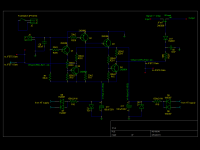
FET 1 and FET 2. Is the feed from V1B AC coupled such that this pont is at zero volts ? If so then both these FET's are tied to ground via the 2M2 and the unmarked resistor. The other side of each FET is AC coupled to the next stage and ground referenced again. So far so good. The gates can be pulled low (to a negative voltage) via the diodes.
FET 5 and 6. Not ground referenced on the output side as drawn ? Where does R19 go ? I'm guessing like the other FET's. That still leaves no ground reference. Add a high value resistor from the output of these FET's to ground.
Mooly, he has potentiometers that provide path to ground, but needs some grid leak resistor. But such rough switching on very sensitive input of guitar amp is something I would never consider.
Yes, but no grid leak. That is what I mean when I say add a high value resistor from output of these FETs to ground.
That is what you mean... yes
")
I understand... Would a small cap in series with the signal path could isolate the control signal from the output?22k is too low resistance. Try something like 2.2 mega ohm or as high as possible, to lower loudness of Thump when switching. This resistor is needed to discharge gate charge, but unfortunately it provides parasitic path for control signal to output. T-configuration as I suggested before would be better in terms of Thumps.
Yep!FET 1 and FET 2. Is the feed from V1B AC coupled such that this pont is at zero volts ?
Oops, sorry for that. The unmarked resistor is 2M2 too!If so then both these FET's are tied to ground via the 2M2 and the unmarked resistor.
Oops again. Yes, R19 is like the other resistors.FET 5 and 6. Not ground referenced on the output side as drawn ? Where does R19 go ? I'm guessing like the other FET's. That still leaves no ground reference. Add a high value resistor from the output of these FET's to ground.
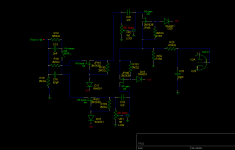
Ok, how about this?
Attachments
By the way, I got in touch with Kevin O' Connor from London Power in Canada. He told me I should have a split-rail control voltage of both polarities, say +/-15 Volts. This would allow the audio signal to live within the control range window...
If by control volts he means the gate drive voltage then I don't agree. Look back at this,
http://www.diyaudio.com/forums/soli...-amplifier-designed-music-11.html#post1569428
It is a similar arrangement to yours. The input is AC coupled and both sides of the FET are ground referenced. As soon as the gate voltage goes above around 0.2 volts (relative to ground) then the FET G-S or G-D junction (depends which way round you have the FET and for these types it really doesn't matter as they are symetrical) will begin to conduct and DC will appear on the output. Just what you don't want. So the positive "on" voltage has to be kept lower than this value. The negative "off" gate voltage has to be more than the peak voltage you are trying to block.
At some point you now have to build the circuit and confirm (or otherwise) that it works as expected
.Yes, I see now. Perhaps there is something I misunderstood. I will build the circuit and get back to you.
By the way, on your schematic I see you have the gate supplied with +/-9 VDC. Isnt it the same thing Mr. O' Connor suggests?
Again, thank you all one more time for the invaluable help and your patience!
By the way, on your schematic I see you have the gate supplied with +/-9 VDC. Isnt it the same thing Mr. O' Connor suggests?
Again, thank you all one more time for the invaluable help and your patience!
By the way, on your schematic I see you have the gate supplied with +/-9 VDC. Isnt it the same thing Mr. O' Connor suggests?
Yes, and I did it to highlight what happens when you increase the gate above around 0.2 volts.
The gate channel begins to conduct for real and to pass current. That gives a DC shift on the output which you don't want. Try it
True, but I think that's where the reverse-biased diode at the gate comes into play.The gate channel begins to conduct for real and to pass current. That gives a DC shift on the output which you don't want. Try it
Anyway, I'll ask him for more details and get back to you, this is very interesting!
True, but I think that's where the reverse-biased diode at the gate comes into play.
Anyway, I'll ask him for more details and get back to you, this is very interesting!
I would have to see it drawn out fully
Your diodes labeled to Vc1 etc (I have assumed) go to the control voltage for the FET. They don't clamp the voltage at all.
Not trying to hijack the thread, but wouldn't a simple diode switch work as well?
The standard switch would introduce transients on turn on and turn off, so use RC delay to slow the switches down.
That's scary
although diode switching works well for RF.I guess a better description would be abrupt turn on which will translate to a step function of the output to the level of the input signal at turn on. I expect this to behave like a transient to the system.
For instance if a clarinet note was at a peak value of 1V at turn on, the drive to the amp would appear as a 1V step function followed by the ensuing sin wave from that value on.
I don't think it would be very pleasant to hear.
For instance if a clarinet note was at a peak value of 1V at turn on, the drive to the amp would appear as a 1V step function followed by the ensuing sin wave from that value on.
I don't think it would be very pleasant to hear.
Attachments
Last edited:
Yessir! Here it is. The second one is what you guys propose.I would have to see it drawn out fully
Attachments

This is how this looks to me at first glance.
In the first one I would say D17 leaves the gate "floating". Imagine +15 volts on the cathode of the diode. The FET is ground referenced at both D and S (as in your circuit). So the diode is non conducting and the gate floats and is liable (guaranteed) to just drift to some voltage determined by leakage paths in the components.
If the diode were substituted by a resistor (say 1Meg) and the diode was now fitted from gate to ground then the diode would clamp the gate to 0.6ish volts. A bit to high. Use a germanium diode and the voltage clamps at nearer 150 to 200 mv. Perfect
Thats how I see the first diagram.
As far as I can see your diagram needs to do the same. The FET's are ground referenced and we need to drive the gate to around 0.2 volts for on and around - 8 volts or more for off.
Build one switch and do some measurements and see
I guess a better description would be abrupt turn on which will translate to a step function of the output to the level of the input signal at turn on. I expect this to behave like a transient to the system.
For instance if a clarinet note was at a peak value of 1V at turn on, the drive to the amp would appear as a 1V step function followed by the ensuing sin wave from that value on.
I don't think it would be very pleasant to hear.
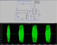
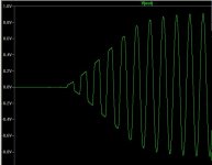
The on waveform looks surprisingly clean I must say. Much better than I would have thought tbh.
Transients and switching a signal at anything other than zero volts causes abrupt changes in levels heard as clicks and thumps. Thats a problem facing any switch, electronic or mechanical.
I will try and build the second one first, since no drilling or much messing with the board is required.Build one switch and do some measurements and see
There are 4 more FETs located at the EQ section, that come from the cathode follower after the preamp which I neglected to show... sorries.
Anyway, I'll try this second topology and let you know.
Thank you again!
- Status
- This old topic is closed. If you want to reopen this topic, contact a moderator using the "Report Post" button.
- Home
- Live Sound
- Instruments and Amps
- JFETs as switch in 2-channel tube amp