How does this buffer work?
@peskywinnets: Do you know about this: http://www.ant-audio.co.uk/Theory/Application_of_Indirect_Negative_Feedback.pdf
@peskywinnets: Do you know about this: http://www.ant-audio.co.uk/Theory/Application_of_Indirect_Negative_Feedback.pdf
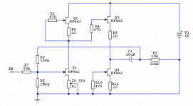
In circuit from post #41 Q3 and Q4 form a CCS loaded Source Follower (search Pass Labs section, B1 buffer).How does this buffer work?
Q1/Q2 form CCS loaded, triode ("Schade") connected common Source gain stage with a gain of 3V/V (set by R6/R7).
Here the original article.Thousands of replies about B1. Could you give me a link, please.
As
said, look for it also in the Pass Labs section of this forum.[...](search Pass Labs section, B1 buffer[...]
Last edited:
... post40 & 41 look like common source to me...
Yes they are - read the second sentence of post #43. It describes the gain stage of both circuits.
I don't understand - in post #43 i wrote that it is a common Source circuit...I have read it again.
I still think I see common source circuits.
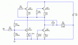
Post #40 doesn't mention a buffer. It shows a circuit that is common-source voltage amplifier (Q1) loaded by CCS (Q2) and wrapped in triode/Schade feedback network (R6/R7) that sets the gain at 3V/V.
Post #41 says that, if need arises, buffer can be added to an existing common-source gain stage and the circuit shows how it's done - Q3 and Q4 are introduced.
Now we come to the obvious mistake in the drawing: there is one wire too much on it, the one that connects lower ends of R4 and R9.
Q3 is a source-follower loaded with CCS (Q4) and together they form a buffer stage.
Both stages (Q1/Q2 common-source gain stage and Q3/Q4 buffer stage) are wrapped in R6/R7 feedback network that sets the gain at 3V/V.
Here is a drawing without a superfluous wire:
Attachments
- Status
- This old topic is closed. If you want to reopen this topic, contact a moderator using the "Report Post" button.
- Home
- Amplifiers
- Solid State
- jfet preamp - does a jfet exist that'll work at just 5V supply?