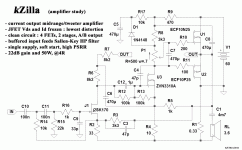
kZilla -- a fetZilla sibling
Hi all,
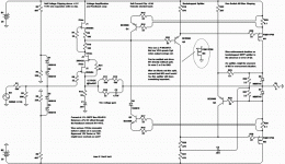
Heavily infected by the fetzilla virus which is most due to its simplicity, I began exploring a variant for single supply and current output, for midrange/tweeter duty. Non-inverting and high-Z input preferred, no DC-coupling.
As luck would have it, this again nicely leads itself to the concept of JFET input and MOSFET VAS as two inverting gain stages. The VAS has to be changed to N-channel, though. This makes it possible to feed identical voltages to the sources, which is sensed AC current plus a small amount of DC coupled voltage. The self-biasing is a bit sketchy but seems to work when both FETs have enough Vgs @ Id to work on.
The JFET load resistor is boostrapped from the VAS source to maintain constant current while constant voltage accross the JFET is achieved by the Vgs of the VAS, which is further multiplied for DC. By this, JFET Vgs also cannot change much in the first place which must lead to low distortion, because the distortion ahead of the very tight feedback loop is factored out. With hot output bias the performance should be truly fantastic from this point of view. The bootstrap capacitor also helps to keep voltages safe during clipping.
The nice thing is now that if we degenerate the bootstrap the voltage accross the load R becomes a linear copy of DC-coupled output voltage leading to a linear current change which is reflected by a square-root Vgs change. The global feedback then changes output current accordingly, but it does not scatter this distortion so in effect it remains almost true 2nd harmonic and completely stationary.
Because of the high voltage gain at DC and LF a 2nd order high-pass is favorable and easy to add as the JFET source is a perfectly buffered input and can feed a Sallen-Key filter. It can in fact be part of the crossover.
PSRR looks really good, output DC is stable vs supply and OK vs temp, as the amp's own DC outputs feeds the bias resistors. Startup is nice with the little helper circuit, but rail-sticking is heavy...
VAS load is only a bootstrapped R, too, and thus VAS current is a slightly distorted copy of output current, but at least on the spice-deck a CCS doesn't make any significant change. I'm about to enter real world with this circuit which will be not easy (HF-style construction required, compensation) but I'm really eager to find out what can be done with only four transistors...
- Klaus
Hi all,
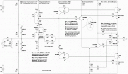
Heavily infected by the fetzilla virus which is most due to its simplicity, I began exploring a variant for single supply and current output, for midrange/tweeter duty. Non-inverting and high-Z input preferred, no DC-coupling.
As luck would have it, this again nicely leads itself to the concept of JFET input and MOSFET VAS as two inverting gain stages. The VAS has to be changed to N-channel, though. This makes it possible to feed identical voltages to the sources, which is sensed AC current plus a small amount of DC coupled voltage. The self-biasing is a bit sketchy but seems to work when both FETs have enough Vgs @ Id to work on.
The JFET load resistor is boostrapped from the VAS source to maintain constant current while constant voltage accross the JFET is achieved by the Vgs of the VAS, which is further multiplied for DC. By this, JFET Vgs also cannot change much in the first place which must lead to low distortion, because the distortion ahead of the very tight feedback loop is factored out. With hot output bias the performance should be truly fantastic from this point of view. The bootstrap capacitor also helps to keep voltages safe during clipping.
The nice thing is now that if we degenerate the bootstrap the voltage accross the load R becomes a linear copy of DC-coupled output voltage leading to a linear current change which is reflected by a square-root Vgs change. The global feedback then changes output current accordingly, but it does not scatter this distortion so in effect it remains almost true 2nd harmonic and completely stationary.
Because of the high voltage gain at DC and LF a 2nd order high-pass is favorable and easy to add as the JFET source is a perfectly buffered input and can feed a Sallen-Key filter. It can in fact be part of the crossover.
PSRR looks really good, output DC is stable vs supply and OK vs temp, as the amp's own DC outputs feeds the bias resistors. Startup is nice with the little helper circuit, but rail-sticking is heavy...
VAS load is only a bootstrapped R, too, and thus VAS current is a slightly distorted copy of output current, but at least on the spice-deck a CCS doesn't make any significant change. I'm about to enter real world with this circuit which will be not easy (HF-style construction required, compensation) but I'm really eager to find out what can be done with only four transistors...
- Klaus
Attachments
Last edited:
Member
Joined 2009
Paid Member
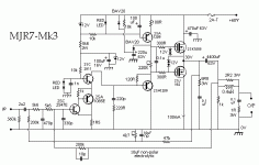
Mike,
Give or take a bit, Stanley's schemat is the one we are using. We will only publish our schemat when we've verified that the new ZVP2110G VAS choice is the cat's meow.
Warning: this may take patience, not for the impetuous.....
Graeme,
Nice to talk again across the years, we must catch up soon, life moves on!!
Because of limitations of loop gain (in this circuit around 55dB) there MUST be a difference between the input and the fb signals which promotes an error signal, which in turn drives the current through the jfet to correct via the VAS.
I'm confident the answer should lie in the maths, but there's no doubt it works well. The variations in gate v. source potential will drive the VAS to place its drain potential at such a value as to reduce the variations to approx the output divided by the loop gain.
I think there will always be errors here because the group delay of the amp will make damn sure the correction is just slightly after the event.
Agree, the perfect fb summing junction would be a virtual earth. Can you do a discrete along these lines?
Nice work, Stanley!!
And a very clever circuit, Klaus, thank you for the fruits of your infection!
Hugh
Give or take a bit, Stanley's schemat is the one we are using. We will only publish our schemat when we've verified that the new ZVP2110G VAS choice is the cat's meow.
Warning: this may take patience, not for the impetuous.....
Graeme,
Nice to talk again across the years, we must catch up soon, life moves on!!
if the signal at the FET source is not =exactly= the same as the signal at the gate then the feedback signal is subtracting from an erroneous version of the input signal and therefore the resulting signal is not properly error-corrected. I imagine the perfect feedback arrangement is a virtual earth summing junction as used in an inverting opamp circuit. What do you think?
Because of limitations of loop gain (in this circuit around 55dB) there MUST be a difference between the input and the fb signals which promotes an error signal, which in turn drives the current through the jfet to correct via the VAS.
I'm confident the answer should lie in the maths, but there's no doubt it works well. The variations in gate v. source potential will drive the VAS to place its drain potential at such a value as to reduce the variations to approx the output divided by the loop gain.
I think there will always be errors here because the group delay of the amp will make damn sure the correction is just slightly after the event.
Agree, the perfect fb summing junction would be a virtual earth. Can you do a discrete along these lines?
Nice work, Stanley!!
And a very clever circuit, Klaus, thank you for the fruits of your infection!
Hugh
Last edited:
Also try adding the 20ohm / 470uF filters
( to the i/p & VAS supply rails )
")
Hi Mikelm,
I have 22ohm + 1000UF rail filters on my PCB. I did not redraw Greg's schematics, I just use M$Paint to change some values.
BTW, I am not using any compensating capacitors (C6 & C13) and the amp seems to be stable.
I found that Farnell stocks ZVP2110A (TO92 version) & I will order that to try out. I am running 20mA thru the VAS and the IRP9610 is only luke warm.
Cheers, Stanley
Hi Hugh,Because of limitations of loop gain (in this circuit around 55dB) there MUST be a difference between the input and the fb signals which promotes an error signal, which in turn drives the current through the jfet to correct via the VAS.if the signal at the FET source is not =exactly= the same as the signal at the gate then the feedback signal is subtracting from an erroneous version of the input signal and therefore the resulting signal is not properly error-corrected. I imagine the perfect feedback arrangement is a virtual earth summing junction as used in an inverting opamp circuit. What do you think?
I'm confident the answer should lie in the maths, but there's no doubt it works well. The variations in gate v. source potential will drive the VAS to place its drain potential at such a value as to reduce the variations to approx the output divided by the loop gain.
I might miss Graeme's original point, but I would think he is saying that this specific error signal, coming from op shift of the JFET, cannot be corrected by even the best feedback loop as it can only compare the output to the "copied" input signal at the source, shifted down by the actual Vgs.
So we must strive to keep Vgs as constant as possible, by locking Vds and Id. My bridge circuit tries to achieve this, even the Vgs change of the VAS due to reflected output load current can be trimmed out to first order. Together with a slight two-pole compensation and partly taking Cdom from the output, this should work out really well even at higher kHz freq and in A/B... sims spit out unbelievable numbers... but even 30dB worse would still be very respectable.
I'm looking forward to find out if the "tube switch" (removing the bootstrap) does what I hope it to do, adding some color, but with control fully maintained.
- Klaus
Last edited:
Actually this question of sound / stabilty / FB & compensation has been in my mind for a few days and I plan to research it with this amp.
I tried to test my amps yesterday for FFT using my new (ish) PC scope and was quite concerned to find quite high levels of distortion . . . then today I measured the FFT of the source signal and that was just as bad so for now I have no way of measuring.
Ah, but I just remember the method Nelson Pass mentioned in an old article where you earth the i/p of amp 1 and play the test signal through amp 2 and through a load resistor into the o/p of amp 1 and put the scope o/p of amp 1 compared to the i/p signal - I'll try that.
I now have two working amps and I'm enjoying listening to music.
Bass is very tight & fast, midrange is smooth and treble seems very clear - not quite as refined and I am aiming for but considering my source, power supply etc at present, it's pretty amazing.
One thing I notice is that it brings out the rhythm and excitement in the music more than any other amps I have had. PRAT in spades !
Now starts a prolonged period of research to optimise.
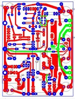
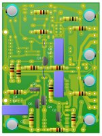
I just about finalised my boards now and will be ordering them before Monday.
There will be a few spare if anyone is interested in my way of building.
They will be £20 / pair & postage.
Now also with possibility for cascoded VAS but no longer with 0.1R o/p degen resistors - only main thing that is not catered for is servo.
Please excuse missing components - in my extremely cheap PCB prog some of the component footprints don't match with my layout and I get fed up with taking them in & out !
mike
I tried to test my amps yesterday for FFT using my new (ish) PC scope and was quite concerned to find quite high levels of distortion . . . then today I measured the FFT of the source signal and that was just as bad so for now I have no way of measuring.
Ah, but I just remember the method Nelson Pass mentioned in an old article where you earth the i/p of amp 1 and play the test signal through amp 2 and through a load resistor into the o/p of amp 1 and put the scope o/p of amp 1 compared to the i/p signal - I'll try that.
I now have two working amps and I'm enjoying listening to music.
Bass is very tight & fast, midrange is smooth and treble seems very clear - not quite as refined and I am aiming for but considering my source, power supply etc at present, it's pretty amazing.
One thing I notice is that it brings out the rhythm and excitement in the music more than any other amps I have had. PRAT in spades !
Now starts a prolonged period of research to optimise.
I just about finalised my boards now and will be ordering them before Monday.
There will be a few spare if anyone is interested in my way of building.
They will be £20 / pair & postage.
Now also with possibility for cascoded VAS but no longer with 0.1R o/p degen resistors - only main thing that is not catered for is servo.
Please excuse missing components - in my extremely cheap PCB prog some of the component footprints don't match with my layout and I get fed up with taking them in & out !
mike
Attachments
Last edited:
more degeneration = less OLG = more stability = sounds smoother
more compensation = more stability = sounds smoother
just sounds like different routes to the same goal to me.
or did I miss something ?
But too much compensation can lead to a flat, lifeless and boring sound.
Such as with these chipamps, they have too much compensation internally that despite low THD and crystal clear sound still make their sound boring in the long term.
Since the last attempt at LTSpice screen capture was utterly unreadable.
We try again with five useless print drivers before finding one that works.
Believe it or not, Microsoft fax driver (win7) looks pretty sharp , open and
edit the .TIFF attatchment (in Irfanview or whatever), don't save draft of
the "message"...
Maybe PDFCreator (sourceforge) would have worked if I had kept at it?
But after a dozen attempts that all look like * warmed in a paper bag.
Upping the dots per inch, .gs still looks like screen capture, not printed.
Same with .png, I gave up experimenting after the msfax driver worked...
This is first time I tried to save an LT image bigger than my screen.
Attachments
Last edited:
- Status
- This old topic is closed. If you want to reopen this topic, contact a moderator using the "Report Post" button.
- Home
- Amplifiers
- Solid State
- JFET input, MOSFET VAS, LATERAL output = Perfect!!