hi sorry i only access to tablet while travelling. circuit draw difficult. very same as the one on your website anyways. mine run with salas bib shunt (x2)
i add snubber to output of shunt, big improvement in hf.
ferrite bead to mosfet gate + 500ohm on output (moosefet preamp inspired), slight improvement in hf
add inductor+ zobel at output, another slight improvement
everything measured with ear only.
surprised psu change most evident because salas shunt already best.
maybe i add 10ohm at the output of shunt.
sounds even more fantastic than before, but mosfet 'glare' still there.
i add snubber to output of shunt, big improvement in hf.
ferrite bead to mosfet gate + 500ohm on output (moosefet preamp inspired), slight improvement in hf
add inductor+ zobel at output, another slight improvement
sounds even more fantastic than before, but mosfet 'glare' still there.
MOSFET "glare" is to with crossover distortion, I've never heard MOSFETs characterised that way in single-ended use before. Indeed, most people find SE MOSFETs sound dark ... probably because the hf is rolled off a little due to the input capacitance and gate resistance.
Anywhow, if you use 500 ohm on output then you use this as a preamp right, not a headphone amp?
yes, use as a preamp. i, too, was expect dark sound, but this is very neutral. straight wire+ little tube distortortion. i think mosfet glare wrong term for me use. high freq just sound little nervous 
maybe since current very high it excite film cap dialectic more? i use polyester cap. when el cap used, sound warm indeed but subdued. film cap bring detail but also glare.
i have ordered russian pio cap. expect to sound very different.
which irfxx0 can i use for even higher roll off? >
maybe since current very high it excite film cap dialectic more? i use polyester cap. when el cap used, sound warm indeed but subdued. film cap bring detail but also glare.
i have ordered russian pio cap. expect to sound very different.
which irfxx0 can i use for even higher roll off? >
Look at the gate charge Qg spec in the datasheet. You can also add a gate resistor / increase its resistance to achieve the same rolloff.
What value polyester cap? For preamp use you can improve the circuit a lot by increasing the source resistance and lowering the value of the output cap.
What value polyester cap? For preamp use you can improve the circuit a lot by increasing the source resistance and lowering the value of the output cap.
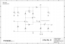
I have finished my JMO-MK II build recently.
It sounds really great. Thank you Richard for the good and interesting project.
Although I am having a bit of background hum noise when connecting it to the Phone or Ipad.
While when using my DAC, either battery powered DDDAC TDA or line powered PS Audio Digital Link II I can not hear the hum.
Will need to investigate it further. Generally the hum can be going from transformer. I have tried to moved signal wires closer and further and it reduces the hum when they are further.
On the other hand it looks like it could be coming from a power strip or lack of grounding in the phone/ipad what do you think it could be.
My grounding is built from a headphone jack directly to the chassis and third pin of the power inlet.
I will upload a picture in a while.
Thanks for your thoughts in advance.
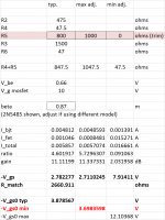
An update, now that I'm able to
measure jfets.
The 2N5486 comes in with a typical turn off voltage (V_gs0) of 3.5 V and beta of 0.9m [measured with R1 1.5k, R2 475]. This is a bit lower than the LTSpice values I based the circuit values on originally.
I'm changing the BOM, the resistor R2 is lowered from 470 ohms to 330 ohms.
No other adjustments are needed. In fact the value of R2 isn't all that critical, it can safely vary from about 150-400 ohms. The lower the resistance, the higher the circuit gain, but the change in gain is not especially wide, ranging from about 11 dB (400 ohms) to about 16 dB (150 ohms).
Attachments
Last edited:
Not necessarily. It depends on the characteristics (pinch off voltage) of the individual jfet you happened to end up with.
With the power off, measure the resistance across the trim potentiometer, pin 1-3, as you have it set currently. If it is above 800 ohms, I recommend reducing R2.
With the power off, measure the resistance across the trim potentiometer, pin 1-3, as you have it set currently. If it is above 800 ohms, I recommend reducing R2.
Let me walk that back.
This circuit is a pain to work with, because all the variables like distortion, gain, and FET characteristics are interrelated.
Short story is the pinch-off voltage (V_gs0) of the JFET defines the optimal circuit gain you need to operate at the lowest possible distortion. It is slightly more than 10/V_gs0. The game runs like "The Price is Right" ... the closer you are to the target value the better, as long as you do not go over.
R2 = 475 is the "better" guess, but it is also the "riskier" guess. There is a higher chance that it is too big for the JFET. If you can adjust the mosfet bias to the proper range using the trim potentiometer, then fine, stay as you are. If you are building the circuit and are not sure what the V_gs0 values are of the JFETs you are using, you are safer using a smaller value.
*****
If you do know V_gs0, or at least estimate it, you can set R2 to an optimal value initially, as
R2 = 1000 * V_gs0 / (10 - V_gs0) ohms.
-- Bob Barker reminds you "Help control the pet population. Have your pets spayed or neutered." --
That formula isn't so accurate.
Here's an excel worksheet that does it better, but I could only do it the reverse direction: input circuit values and output the appropriate V_gs0, so if you know the V_gs0 you have to play around with different values of R2 until you get the output value of V_gs0 close to the jfet you have.
Cut-to-the-chase,
R2 = 475 ohms, minimum V_gs0 3.7 V
R2 = 330 ohms, minimum V_gs0 3.0 V
About half of the 2N5486 I measured the other day appear to be too low to work at 475 ohms. The J-Mo II I built some while back worked fine though, so either I got lucky or maybe I'm overthinking this.
Attachments
I'm not familiar with it. If your tester can measure JFET pinch off voltage it's all good. Some of the simple circuits for jfet matching on the web actually measure V_gs at some nominal current and not the pinch off voltage.
Or, this works.
Or, this works.
http://www.peakelec.co.uk/acatalog/dca75-dca-pro.html
This what I have.
Sent from my iPhone using Tapatalk
This what I have.
Sent from my iPhone using Tapatalk
That's the one I'd recommend for this job, yes. I was going to buy one myself, but I already have a BJT tester and honestly I already have the equipment to do the same kind of curve traces if I put my mind to it. The only downside to the DCA-75 is it only measures quite small currents, and, iirc, up to about 12 V or so.
- Status
- This old topic is closed. If you want to reopen this topic, contact a moderator using the "Report Post" button.
- Home
- Amplifiers
- Headphone Systems
- J-Mo Mk II headphone amplifier