Hi, this is a continuation of my thread for XO/HPF combo unit with associated PSU (see sig).
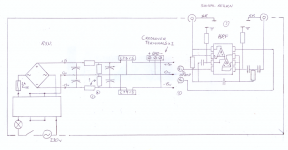
The PSU and XO sections are working fine - but I'm left with humming in HPF section. Nearby transformer is not the cause because the XO works splendidly.
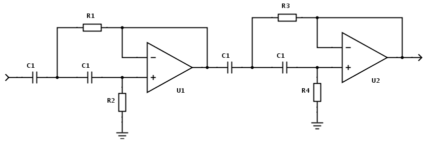
Currently in doubt about how some parts of circuit are connected - For ease I've circled 3 doubts on below schematic with questions.
I hope its these that are causing the problem.
It is a relatively simple circuit.
Refer to schematic for numbering:
1. How should the filter resistors be orientated (I currently have them horizontally, this could be wrong).
2. How should the op-amp V+ and V- terminals be connected relative to the PSU?
3. As you can see i'm left with four unterminated 'commons', 2 are signal returns, and 2 from the hpf circuit - I don't know how to connect these or if they should be left like this.

Thanks in advance

The PSU and XO sections are working fine - but I'm left with humming in HPF section. Nearby transformer is not the cause because the XO works splendidly.
Currently in doubt about how some parts of circuit are connected - For ease I've circled 3 doubts on below schematic with questions.
I hope its these that are causing the problem.
It is a relatively simple circuit.
Refer to schematic for numbering:
1. How should the filter resistors be orientated (I currently have them horizontally, this could be wrong).
2. How should the op-amp V+ and V- terminals be connected relative to the PSU?
3. As you can see i'm left with four unterminated 'commons', 2 are signal returns, and 2 from the hpf circuit - I don't know how to connect these or if they should be left like this.
Thanks in advance
Attachments
I completed a 3way active speaker with 2ways in one box and a separate 1way for the bass only.
In the mid and treble box attached to the back of a small (5"+1" drivers) speaker I have a high pass filter and a bandpass filter as well as two chipamp channels & PSU. The Chassis is only 163x155x68mm, less that 1.7litres. It's all crammed in pretty tight.
I attached the input RCA directly to the chassis back panel. Expecting to have to change it after failed testing. But no measurable hum, no increased noise. It seemed to work !
Last edited:
Forget about commons and grounds and other confusions.
EVERY signal is transmitted via a PAIR of wires. There are no exceptions.
Identify the pair of wires in every connection and twist them. solder at the 4 terminations.
The dual polarity PSU appears as an exception, but it is two 2wire connections where one wire carries the two return signals. We can return that signal as PSU Zero Volts. The two sets of 2wires becomes a twisted triplet.
Last edited:
Find the connection for the input signal.Identify the pair of wires in every connection and twist them. solder at the 4 terminations.
It must be 2 (two) wires.
The two wires have four ends. Solder these four ends to the respective terminals.
The input socket gives you two terminals. The Receiver PCB has two input terminals. Solder to those four terminals.
Repeat for EVERY connection.

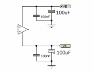
You didn't show any PSU to op amp power pin bypass supply caps. That might account for noise.
Certainly. Also there must be 10uF capacitors right at both regulator outputs.
Did nobody read my op - I did try to keep it as simple as possible
I've labelled diagram 1,2 and 3. These are uncertainties which I think may be the cause.
(3) Connecting up commons
Andrew, in the diagram, I've labelled S.R. (Signal Return) at the top right of the diagram. The left circle/jack is the output and the right jack is input, as you can see each already has two connections protruding...
In my previous post in that attachment is my interpretation of your instructions.
I connected SR to SF for both. Is this right?
(2) connecting HPF to PSU
Shred spread and rayma,
I want to start with some clarity on how commons should be connected.
Only if problem persists, will I add more caps...
What does remain unclear with PSU however is how (single polarity) + and - HPF connects to the (dual polarity) PSU?
This could very well be causing the hum. I can't recall how I have it currently connected - that's why I've left everything un-connected in diagram.
(1) Orientation of filter resistors
Last but not least, how should filter resistors be connected relative to filter caps? Currently they are in series to caps, I fear they should be connected/orientated the other way vertically (see diagram) judging by alot of PSU circuits I've seen online...
Last edited:
Did nobody read my op - I did try to keep it as simple as possible
I've labelled diagram 1,2 and 3. These are uncertainties which I think may be the cause.
(3) Connecting up commons
Andrew, in the diagram, I've labelled S.R. (Signal Return) at the top right of the diagram. The left circle/jack is the output and the right jack is input, as you can see each already has two connections protruding...
In my previous post in that attachment is my interpretation of your instructions.
I connected SR to SF for both. Is this right?
A close coupled pair is TWO WIRES or TWO TRACES right next to each other.I can't see any close coupled Flow and Return wire pairs in the pic you posted.
Ok, I looked around online to see if I can perhaps find a schematic to help me.
I found this one below. For some reason, for 24dB/oct this circuit features (more) op-amps.
Are the input buffer and line driver stages really necessary?
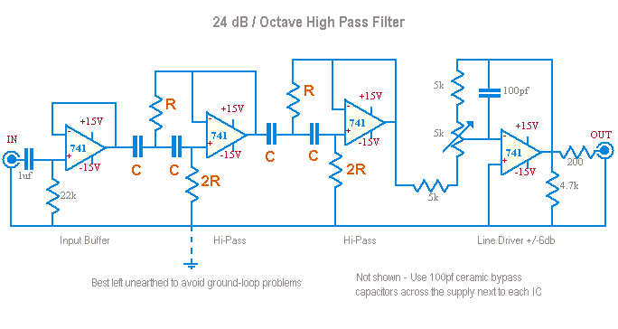
The design I'm using only features one (dual) op-amp. It easy to see how why I find electronics so confusing!
@ jeffremus. As tempting as it is, I'd much prefer mains powered device.
I found this one below. For some reason, for 24dB/oct this circuit features (more) op-amps.
Are the input buffer and line driver stages really necessary?
The design I'm using only features one (dual) op-amp. It easy to see how why I find electronics so confusing!
@ jeffremus. As tempting as it is, I'd much prefer mains powered device.
An externally hosted image should be here but it was not working when we last tested it.
Last edited:
Let's use the upper pic to explain.
The input is the IN label on an RCA style socket.
The Hot Signal is the filled in Dot. The signal Return is the part circle around that Dot.
Here the signal Flow and return are close coupled. Even Better the Return forms a screen around the Flow.
The Flow comes out to feed a Capacitor. Then it feeds a wire to a resistor then it feeds a wire to the +IN
The return follows a different route. Upto the resistor it has a big loop. Eliminate that loop by running a twisted pair to the resistor. From the resistor run a twisted pair to the +IN. Solder the Flow to +IN.
Where does the Return go?
The Signals Flows through the chip. The Return trace or wire must follow along the chip package then alongside the string of capacitors then along the next chip ... etc ... to the output of the final chip. Now a twisted pair to the 4k7. Then a twisted pair to the 200r resistor. Then a twisted pair to the output socket.
This way you are forcing the Return current to flow as closely as possible to the ROUTE that the Flow signal takes from input to output. This is close coupling.
It applies between equipment boxes. It applies between modules inside a box. It applies across a signal handling PCB.
Next, look at all the loops that makes the schematic clear and easy to read.
These MUST be made small, i.e. close couple the return route to the flow route.
Take the 22k at the input, as shown you would split the twisted pair to feed the two ends. = loop area. out from the resistor you have a split pair that becomes a twisted pair = loop area.
Two avoidable loop areas.
Instead lay the 22k resistor along parallel to and directly over the Flow Trace.
attach the twisted pair so that it uses the resistor + underlying trace as PART of the CLOSE COUPLED PAIR. You eliminate two loops.
Last edited:
Alright, I've read your instructions thoroughly... Please forgive me if this is not right... Hopefully atleast partially right.

It seems to be in line with an observation I made, when the Return is shorted to the upper side of 2R - this eliminates the hum... when return is connected to the bottom side of 2R, hum is present.
It seems to be in line with an observation I made, when the Return is shorted to the upper side of 2R - this eliminates the hum... when return is connected to the bottom side of 2R, hum is present.
It seems to be in line with an observation I made, when the Return is shorted to the upper side of 2R - this eliminates the hum...
when return is connected to the bottom side of 2R, hum is present.
This is wrong, you're grounding the positive inputs and altering the entire circuit operation.
- Status
- This old topic is closed. If you want to reopen this topic, contact a moderator using the "Report Post" button.
- Home
- Source & Line
- Analog Line Level
- Hum issue in hpf circuit