Pierre said:Ledmania.
Let me clariry the concept of NFB (negative feedback) a little bit...
(Negative) Feedback is used to sample a portion of the output and compare it to the input so any deviation (well, not any, but to some extent determined by the loop gain, bw, etc), can be corrected by generating an "error" signal that is the real input to the PWM amplifier.
Clock based Class-D amps can implement feedback (it's not something exclusive of self-oscillating ones, for god's shake!!!), and in fact they do. I have tested about 8 different variations of PWM amplifiers and all of them use feedback. Some of them before filter, others after it. The fact is that they sound much better that in open loop. (In fact I wouldn't even think on building an open loop PWM amplifier, specially with a PWM chip!!)
Lumanauw: Feedback can (I would say MUST) be implemented with a chip like SG3525.
Hi Pierre,
Im so sorry for offending you on my last post but I have no intetion of opposing your idea of implementing fb
") . As I have said on my last paragraph that you can put it as you like but I suggest it would be more practical to put it after the filter. I'd been contemplating for quite a while now in digging the advantage of using high frequency fb but my mathematical capability is not enough to cope with that concept so why to bother on that route while there is a more simpler solution that my IQ can grasp? When I'm designing any class d amp, I am just treating it as a convetional linear amp in implementing fb. I use the old concept of either DC fb or AC fb but on the audio spectrum only.
. As I have said on my last paragraph that you can put it as you like but I suggest it would be more practical to put it after the filter. I'd been contemplating for quite a while now in digging the advantage of using high frequency fb but my mathematical capability is not enough to cope with that concept so why to bother on that route while there is a more simpler solution that my IQ can grasp? When I'm designing any class d amp, I am just treating it as a convetional linear amp in implementing fb. I use the old concept of either DC fb or AC fb but on the audio spectrum only. As in the sg3525 I admit that I did not put any fb nor any filter on it
b'coz it is only a prototype. Remember that a "working" proto with a incomplete components but produce nice sound will double its nice factor when you complete the required components.
Cheers
ledmania
No offence at all!!
From your last sentences, I think you have things a bit more clear than you think. I was not thinking on concepts such as "high frequency" feedback, but feedback in the audio band, as you say.
In fact, feedback is usually implemented so the crossover frequency (the one where loop gain is below 0dB or 1v/v) is less than half the switching frequency. The goal is to provide feedback within the audio band, where it is useful for reducing distortion.
And yes, it is better in terms of linearity to take feedback after the filter, but more difficult and dangerous in terms of estability. Usually, taking it before filter is enough. As it is integrated in the error amplifier, the high frequency content is attenuated.
The process of designing feedback in Class-D is about the same as in any other type of amplifier, with the exceptions that you have to account for the LC filter phase shift if you take after it.
But there are some other things to solve before imlementing feedback. The amplifier must work as good as possible in open-loop, and then the way to go is trying to optimize its performance with NFB. There is no point in trying to "save" a system that is very bad performing in open-loop.
Please let's go on with the original discussion (trying to establish a starting point of Class-D design basing on PWM controller chip and keeping it as simple as possible while still performing good)
Pierre said:But there are some other things to solve before imlementing feedback. The amplifier must work as good as possible in open-loop, and then the way to go is trying to optimize its performance with NFB. There is no point in trying to "save" a system that is very bad performing in open-loop.
[/B]
Perfect point!!!
This is the main reason why I am permanently nailed on using those chips ever since I tried and tested it for more than two years now. Since those chips are cheap in prices, some of its many advantages over their discrete counter part are; higly stable, built in soft start(no "thump" sound during start up), built in high quality comparator, programable oscillator up to 1mhz are common.
Mind you, I abuse mine with lots of dangling wires and jumpers everywhere but it still insist to produce nice sound with good waveform on my oscilloscope. Actually, I tested 5 chips already and majority of them are working fairly identical in sound but your finall decision will reflect on choosing additional features like over current protection and etc. etc..
One interesting point I want to emphasize on this thread is that the use of PWM controller chips which was spicificaly "intended" by the chip maker for DC to DC converter applications is now playing your favorite music inside a small aluminum box is a"very"rewarding experience that a hobbyist may ever encounter
Pierre said:Please let's go on with the original discussion (trying to establish a starting point of Class-D design basing on PWM controller chip and keeping it as simple as possible while still performing good)
[/B]
I'll obay!
cheers
Ledmania.
I think that features like overcurrent protection, soft start, etc, in these chips are useless (and even harmful) when using them with mosfets to create relatively high output powers (more than 1W or so ). The reason is that you want the chip to be oscillating at 25% duty cycle (each output) in order to have a symmetric square bipolar output and hence 0V after the filter. If you turn the PWM off by means of the overcurrent protection, shutdown or similar, you will get 0% duty cycle in each output. Remember that you join them in order to have a single PWM signal, that then you must invert to create the LS and HS drives. Then one of the mosfets will be permanently off while the other is permanently on (ok, if the "on" one is the highside it will be turned off after a while due to bootstrap cap discharge with no oscillation). That's something you really don't like!
So: in order to build a useful Class-D amp out of these chips, you need to be sure that soft-start, overcurrent, shutdown, overvoltage, undervoltage or whatever protections or features it have, don't engage, unless you have the power stage disabled, or you will get a large DC at the output, burning your speakers in the worst case.
The only function of this chip you need is the PWM modulator and error amplifier (although ledmania doesn't like this one). So choosing a chip basing on this features is an error. The only parameters that should make a decision are speed, linearity, maximum duty cycle, and output configuration.
Best regards.
I think that features like overcurrent protection, soft start, etc, in these chips are useless (and even harmful) when using them with mosfets to create relatively high output powers (more than 1W or so
). The reason is that you want the chip to be oscillating at 25% duty cycle (each output) in order to have a symmetric square bipolar output and hence 0V after the filter. If you turn the PWM off by means of the overcurrent protection, shutdown or similar, you will get 0% duty cycle in each output. Remember that you join them in order to have a single PWM signal, that then you must invert to create the LS and HS drives. Then one of the mosfets will be permanently off while the other is permanently on (ok, if the "on" one is the highside it will be turned off after a while due to bootstrap cap discharge with no oscillation). That's something you really don't like!So: in order to build a useful Class-D amp out of these chips, you need to be sure that soft-start, overcurrent, shutdown, overvoltage, undervoltage or whatever protections or features it have, don't engage, unless you have the power stage disabled, or you will get a large DC at the output, burning your speakers in the worst case.
The only function of this chip you need is the PWM modulator and error amplifier (although ledmania doesn't like this one). So choosing a chip basing on this features is an error. The only parameters that should make a decision are speed, linearity, maximum duty cycle, and output configuration.
Best regards.
Hi Pierre,
Why dont you use LM3524 from National semiconductor which is very much faster than SG3524 and it is a very low cost solution also....
Since the motive behind the project is simplicity and low-cost and implementing it using LM3524 + IR2110 in Sub-woofer application is a very ergonomic[Human friendly] way.....
regards,
K a n w a r
From the datasheet, I see that LM3524 is just as slow as SG3524 (typ 200/100ns rise/fall times). But it does have an advantage: its output transistors are rated to 60V, so perhaps they can do the level shifting with no additional transistors...
I am sure that any of these PWM controllers will do OK for subwoofer use, what I was trying to see if it can be improved to full-range use with hi-fi performance by choosing a different (unfortunately more expensive) PWM chip.
Best regards,
Pierre
I am sure that any of these PWM controllers will do OK for subwoofer use, what I was trying to see if it can be improved to full-range use with hi-fi performance by choosing a different (unfortunately more expensive) PWM chip.
Best regards,
Pierre
Pierre said:From the datasheet, I see that LM3524 is just as slow as SG3524 (typ 200/100ns rise/fall times). But it does have an advantage: its output transistors are rated to 60V, so perhaps they can do the level shifting with no additional transistors...
I am sure that any of these PWM controllers will do OK for subwoofer use, what I was trying to see if it can be improved to full-range use with hi-fi performance by choosing a different (unfortunately more expensive) PWM chip.
Best regards,
Pierre
Hi Pierre,
Yes ofcourse, if you want something fast than try this combination....
erroramp=OPA627
very high speed Differential comparator = LM360
Precision Triangle generated through combination of Crystal Oscillator using CD4060 counter and high speed integerator using LM6172 opamp.....
Low Gate Charge Mosfets from APT= APT30M18LVR ~Tgc=50nC
regards,
K a n w a r
Pierre,
you are mistaking in disregarding the important features of the chip. In fact the soft start features is well advisable in all audio apps to eliminate the turn on "thump" in which most of diyaudio members are complaining about. When you try to start the chip with soft start capacitor in placed, and your oscilloscope probe is connected to the output, you will notice that the signal will gradually start from 0%duty then stop on 50% at slow incremental rate. I'd been designing linear amps for 27 years now but the oldest technic that we put to aviod thump is to use relay. Been there done that,all I can say is SS is as important as current protector.
As with the over current protection, most high end amp is equipt with this features. Take note that not all amps are "idiot proof". this means in one way or another it may encounter accidental output short circuit like in bar b-Q party with the speaker cables are lying around .
Its nice to hear that you will try those chip to use as class d amps. I'll tell you...You will like their sound. But when you use them and disregard their SS and over current features then you are five steps forward but moved to six step backward.
BTW, the 25% duty cycle that you metioned is applicable only to the chip that is "double ended push pull" converter that we are talking about. Each two o/p should be 25% each, then mixed them with the added two diodes plus pulldown resistor to convert them into "single ended topology".This way, those 25%will become 50%.
As I mentioned to you on my first post that I already tried at least 5 chips since last 2 years and two of them are for "single ended topology" that eliminates the two diodes and resistor all together. the o/p can be adjusted from 0 to 98% and they sound nice too.
Hey Pierre, are you stil awake?
thanks for not yawning
you are mistaking in disregarding the important features of the chip. In fact the soft start features is well advisable in all audio apps to eliminate the turn on "thump" in which most of diyaudio members are complaining about. When you try to start the chip with soft start capacitor in placed, and your oscilloscope probe is connected to the output, you will notice that the signal will gradually start from 0%duty then stop on 50% at slow incremental rate. I'd been designing linear amps for 27 years now but the oldest technic that we put to aviod thump is to use relay.
Been there done that,all I can say is SS is as important as current protector. As with the over current protection, most high end amp is equipt with this features. Take note that not all amps are "idiot proof". this means in one way or another it may encounter accidental output short circuit like in bar b-Q party with the speaker cables are lying around
.Its nice to hear that you will try those chip to use as class d amps. I'll tell you...You will like their sound. But when you use them and disregard their SS and over current features then you are five steps forward but moved to six step backward.
BTW, the 25% duty cycle that you metioned is applicable only to the chip that is "double ended push pull" converter that we are talking about. Each two o/p should be 25% each, then mixed them with the added two diodes plus pulldown resistor to convert them into "single ended topology".This way, those 25%will become 50%.
As I mentioned to you on my first post that I already tried at least 5 chips since last 2 years and two of them are for "single ended topology" that eliminates the two diodes and resistor all together. the o/p can be adjusted from 0 to 98% and they sound nice too.
Hey Pierre, are you stil awake?
thanks for not yawning
Let's try to clarify the confusion
.
I fully agree in that soft-start, overcurrent, etc in an amplifier are mandatory, I was only saying that the on-chip features are not suitable for a double-ended topology with push-pull, where 25+25% duty-cycle is required and hence a variation from 0% will produce a negative output progressively going up to 0% where the circuit regulates properly at 25+25%=50%.
From what I can see in your schematics, you are using ONLY one of the outputs of the SG3524 (the collector of the upper output, pin 12 is tied to GND, so you are deactivating that output and using only the lower transistor, you are really wasting a diode).
That setup won't work when trying to implement a power stage for it, as your duty cycle only varies from 0 to 45-50%, and you really need it to vary symmetrically (0 to 100% or 10 to 90% for example) in order to implement a half bridge and DC couple the output as usual.
I don't know if you understand me, Ledmania. I am not saying that the circuit doesn't work for you, but we are trying to buid a High power class-D so the mosfet stage is needed and your circuit can't be used as it is for that.
If the way you combine your double outputs is different, then what I say doesn't apply. If you could show us
Pierre said:Let's try to clarify the confusion
From what I can see in your schematics, you are using ONLY one of the outputs of the SG3524 (the collector of the upper output, pin 12 is tied to GND, so you are deactivating that output and using only the lower transistor, you are really wasting a diode).
That setup won't work when trying to implement a power stage for it, as your duty cycle only varies from 0 to 45-50%, and you really need it to vary symmetrically (0 to 100% or 10 to 90% for example) in order to implement a half bridge and DC couple the output as usual.
No pierre, maybe you are looking at the wrong drawing. Take a look at it once more and you'll see that I used sg3525 double ended totempole output but not sg3524 with open emiter/collector output. as I said earlier that this sg3525 was tested by myself by loading it with a headphone.
I just show to you and to lumanauw that this is one of many chips that is possible to use as primary stage class d source.
Of coarse you have to provide additional amplification and levelshifting on this part like the use of IR2011 as the driver for power fets.I did not include the HI/LO side fet driver assembly because I know that majority of the readers of this thread already know that circuit configuration
Pierre said:
I don't know if you understand me, Ledmania. I am not saying that the circuit doesn't work for you, but we are trying to buid a High power class-D so the mosfet stage is needed and your circuit can't be used as it is for that.
My answer is same as above...
Regards
Sorry, Ledmania. I though it was an SG3524.
OK, if your sch. shows an SG3525, the outputs are push-pull and then they are connected OK (wired OR with diodes and pulldown).
But what I was trying to point out is that it works for you with shuwdown, slow start and all that stuff because you are AC coupling the output directly: at starts, output increases from 0 to 50%. At 50% (that you have pre-adjusted), you have VCC/2=6V at the output, but as you have a coupling cap, no problem. So the effect will be your coupling cap slowly charging and hence no turn on "pop". (without that slow start, you would get the same effect as with old Class-AB amplifiers that used unipolar supply, that kind of nasty "thump!")
So we agree so far...
...BUT in the right moment that you use this chip in conjunction with a power stage, that it is all DC coupled: steady state corresponds to 50% duty cycle, that produces 0V at the output. 0% means -VCC (-50V or whatever) at the output, and 100% means +VCC (+50V or whatever). SO if you use slow start, your output will start at -50V and then will rise to the final point of 0V (assuming no input signal). And that's NASTY, believe me!
The same applies with overcurrent: you can implement a circuit at the power stage that detects overcurrent, but it should shutdown the power stage (IR211X chip or both of its inputs), but NEVER the PWM chip, as it will go to 0% duty cycle which equals -VCC at the output, burning your speaker!
Conclusion: PWM chips CAN be used for Class-D half bridge designs, but several questions must be had in mind, such as WHERE to implement slow-start and overcurrent, as well as feedback. We will try to build a high-power one based on SG3525 (or UC3825 for better fidelity)
I hope eveything is now clear from my part and also from yours.
Best regards,
Pierre
Pierre said:Sorry, Ledmania. I though it was an SG3524.
OK, if your sch. shows an SG3525, the outputs are push-pull and then they are connected OK (wired OR with diodes and pulldown).
But what I was trying to point out is that it works for you with shuwdown, slow start and all that stuff because you are AC coupling the output directly: at starts, output increases from 0 to 50%. At 50% (that you have pre-adjusted), you have VCC/2=6V at the output, but as you have a coupling cap, no problem. So the effect will be your coupling cap slowly charging and hence no turn on "pop". (without that slow start, you would get the same effect as with old Class-AB amplifiers that used unipolar supply, that kind of nasty "thump!")
So we agree so far...
It's nice that you see the correct sch. Take note that my sch was intended only to verify the validity of the chip to use as class d source thats why I put coupling caps on the o/p to isolate the dc supply through the head phone as the load.This is my old technic in verifying such audio circuit:breadboard+scope+headphone.I dont have cuircuit simulator yet.But in real world of application the coupling cap must be remove then the output of the chip must be split into two via inverter (just same as your PDF sch).
Pierre said:
...BUT in the right moment that you use this chip in conjunction with a power stage, that it is all DC coupled: steady state corresponds to 50% duty cycle, that produces 0V at the output. 0% means -VCC (-50V or whatever) at the output, and 100% means +VCC (+50V or whatever). SO if you use slow start, your output will start at -50V and then will rise to the final point of 0V (assuming no input signal). And that's NASTY, believe me!
The topic is becoming more interesting.
I understant your point Pierre, and I think I have a solution for that initial logic "0" at 0% duty. You are correct that the speaker may encounter instant "pop" even the ss is at work.
First, Lets use your PDF sch because it is the most typical to most readers and is available now.
Since you use inverter at the output of the "OR" diodes to split the signal in a complementary fashion for hi/lo side of fet driver, My solution is to change that inverter with inverter also but with "TRI state" feature. Remember that IR2xxx drivers has a safety faeture of always at logic "0" on both o/p at start up unless a signal is comutated on its input. This logic "0" on both output of IR2XXX will corespond to both "off" on o/p of the power fets.
Take note that when the o/p of the two power fets are "off" it means they are at "TRI state" also and not negative. You will measure at the o/p a very small leakage current comming from the driver because of the isolation barrier on the driver and not the power fets itself.
Now, this control pin of the tri state inverter must be connected to the o/p of UC3XXX with proper RC filter to accept only plain DC.
BTW,the inverter must be "schmit inverter" so that it will respond in a sharp "knee" of hyterises to the RC filter input.
I hope you got my point
Pierre said:
The same applies with overcurrent: you can implement a circuit at the power stage that detects overcurrent, but it should shutdown the power stage (IR211X chip or both of its inputs), but NEVER the PWM chip, as it will go to 0% duty cycle which equals -VCC at the output, burning your speaker!
I have a solution on this issue also but lets finish the SS issue first
If there are someone on this forum who will respond on my idea above then this will be a very healthy and informative discussion.
Pierre said:
Conclusion: PWM chips CAN be used for Class-D half bridge designs, but several questions must be had in mind, such as WHERE to implement slow-start and overcurrent, as well as feedback. We will try to build a high-power one based on SG3525 (or UC3825 for better fidelity)
I hope eveything is now clear from my part and also from yours.
Best regards,
Pierre
I think this is the only begining of a healthy and informative discussion regarding.............
""PWM chips CAN be used for Class-D half bridge designs, but several questions must be had in mind, such as WHERE to implement slow-start and overcurrent, as well as feedback. We will try to build a high-power one based on SG3525 (or UC3825 for better fidelity)""
CHEERS
ledmania.
For slow start, I have also though on using tri-state inverters followed by pull-downs. Once you have a control pin (the OE of that chip), you can put a RC network, so at startup the voltage at that control pin is initially 12V and it decreases until it reaches the threshold and activates the OE and hence both inputs to the IR211x at the same time.
That input can also be used for other protections.
That input can also be used for other protections.
Pierre said:For slow start, I have also though on using tri-state inverters followed by pull-downs. Once you have a control pin (the OE of that chip), you can put a RC network, so at startup the voltage at that control pin is initially 12V and it decreases until it reaches the threshold and activates the OE and hence both inputs to the IR211x at the same time.
That input can also be used for other protections.
Thanks for favoring the idea.
At this type of function, the over current protection on the chip can also share the use of this tri-state features.
But you know Pierre, when I was eating my lunch a while ago, there is somthing that bothers my mind. This is base on the SS that we want to implement. I have noticed that if the tri-state was used, and the SS cycle has just completed maybe it will return again to its original "thump" sound because of the output is now 1/2VCC again

maybe the overcurrent will only benefit from this but not the SS.
But try and try until we succeed.
Cheers
Sorry, I don't understand your estatement.
We will use bipolar supplies. Assuming that the chip slow-start is fast enough, it will reach 50% duty cycle (combined output of both outputs of the chip), that corresponds to 0V output. _ After_ that, the inputs to the IR211x chip are enabled (by means of the tri-state control), and it starts oscillating. I think that won't produce noise...
We will use bipolar supplies. Assuming that the chip slow-start is fast enough, it will reach 50% duty cycle (combined output of both outputs of the chip), that corresponds to 0V output. _ After_ that, the inputs to the IR211x chip are enabled (by means of the tri-state control), and it starts oscillating. I think that won't produce noise...
phase_accurate said:I think the soft-start can be overridden anyway.
Regards
Charles
LOL!!!
I want to think of that too but taxing my brain to solve this puzzle will surely make me more jubilant if we hit the bulls eye..Cheers
ledmania
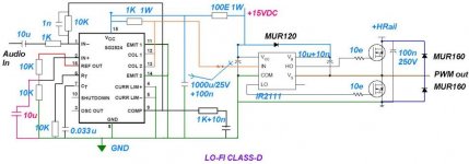
Some comments for Kanwar.
Your schematics is for only a section of a full-bridge amplifier, isn't it? If not, your output must be AC coupled, or there will be a +HRail/2 DC component at the output. (and AC coupling at the output is something we really don't like in high power amplifiers)
You don't use feedback as well, that would be very nice and I think it won't be difficult to achieve.
Best regards,
Pierre
- Status
- This old topic is closed. If you want to reopen this topic, contact a moderator using the "Report Post" button.
- Home
- Amplifiers
- Class D
- How to fix this sch?