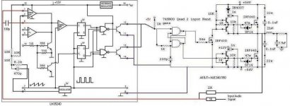
I think that the simplicity of the first sch, the Class-D design, should encourage us to try to complete it, at least to give it a try (it is obvious that the circuit is not well drawn, but some things can be fixed easily).
The oscillator cap and res (pin6 6 and 7) must go to the GND reference of the SG3524 chip. The thing is, did the author want to reference it to -56V rail? If so, the only level shift required for the PWM signal is for the high side. But in that case, a capacitive coupling of the input is mandatory, and I can't see it, so I think that its reference is GND, so there is an error.
The driver stage has NPN/PNP drivers. That's good, but the lower one should be fed at +12V referenced to the negative rail, which is not clear in the sch. And the high side one has a bootstrap diode+cap, but the diode anode should go to that same +12V supply, not to the +56V rail, unless there is a 12V zener in parallel with the bootstrap cap to prevent overvoltage.
The level shifting part is not clear. If the input stage is referenced to GND (it should be), level shifting is required for both parts (HS and LS).
That's easy to fix, we can use a PNP for the LS drive, but that's a bit more difficult for the HS part.
Another thing that worries me is the capability of SG3524 chip to generate a 0 to almost 100% PWM (from what I know it goes from 0 to 45% at each output, although this is wired a bit different in this sch...)
Where did you find this. Do you have any evidence that a variation of this circuit is working anywhere (it is obvious that it can't as it is drawn)
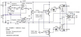
About the second circuit, the PWM modulator is quite straightforward, and the power conversion circuit is very similar to a DC/DC push-pull inverter, with buffered gate drivers.
The "secondary" part uses the transformer inductance in combination with the .1uF capacitor as the output filter.
However, due to the imperfections in the transformer (leakage inductance producing spikes, and its output going int o discontinuous mode, etc, I doubt this can produce an accurate representation of the input signal... unless someone demonstrates the opposite, of course!
Hi, Pierre,
I found this on a member's website, Dan Fraser.
Do you think the first one (SG3524) based is more likely to work? I also think the same thing, because in the second one, there will be not-balanced magnetic flux on the transformer, will make it hot or saturated.
I wanted to build a lo-fi subwoofer amp, no need to be hi-fi, just be loud enough and runs cool And because it is for lo-fi subwoofer, maybe the oscilating frequency can be below 100khz or even below 50khz? (to fit the IC's purpose, usually SMPS IC's works below 100khz)
If the T-on is not close enough to 50% (just 45% like you said), I think it's OK for my application, it wont be a hi end piece.
About the T-on. Is it better to use TL494 to get T-on closer to 50%?
But....will it work AT ALL?
I found this on a member's website, Dan Fraser.
Do you think the first one (SG3524) based is more likely to work? I also think the same thing, because in the second one, there will be not-balanced magnetic flux on the transformer, will make it hot or saturated.
I wanted to build a lo-fi subwoofer amp, no need to be hi-fi, just be loud enough and runs cool
And because it is for lo-fi subwoofer, maybe the oscilating frequency can be below 100khz or even below 50khz? (to fit the IC's purpose, usually SMPS IC's works below 100khz)If the T-on is not close enough to 50% (just 45% like you said), I think it's OK for my application, it wont be a hi end piece.
About the T-on. Is it better to use TL494 to get T-on closer to 50%?
But....will it work AT ALL?
Lumanauw,
You may definitely give a try to the first circuit, but don't waste your time with the second one. But even that needs some modifications to start its basic operation.
I have to think more about it (there are people much more capable in this forum anyway), but the problem with SG3524 is not that it doesn't reach 50% (the only problem with that is that it won't swing to the supply rails, but that has its advantages also, as it won't never stop oscillation at clipping). What really worries me is the SG3524 output arrangement: I need to draw the waveforms in order to see if that resembles the required PWM format. Perhaps.
Another point to take care of are the level shiftings. I would modify that so the SG3524's PWM output is ground referenced. Then level-shift it so it swings between -56V and 12V above that (-44V). Then you can need to have it level shifted for the HS driver:
The second level shifter could be something like that:
Use a NPN transistor (rated at 150V at least). PWM (after first level shift) goes to base. Emitter goes to -56V with a 1k resistor. Collector goes to bootstrap voltage via a 1k resistor. Output of the level shifter is taken from collector, and then to the NPN/PNP HS driver.
Note that this arrangement is inverting, so you don't need additional inverters. The first level shift also inverts, so in fact you don't need any inverter.
The bootstrap voltage can be easily obtained: 10uF capacitor negative terminal goes to mosfets midpoint (bridge output). Positive terminal is fed from +12V (referenced to GND) via a schottky diode. The join point supplies 12V referred to HS mosfet source and that's all.
I have been thinking and writing at the same time, so please post your comments or questions if something is not clear or wrong.
Hi Lumanauw,
Use SG3524 + IR2111 + 2 X IRFP250N
and you have very simple but an effective good quality Class-D amp, because i have tried it and made it for a subwoofer...
Set the Oscillator frequency around 40KHZ, wire the open collector outputs of PWM IC in "OR" configuration i.e. join the collectors together and add a pull up resistor of 1K to +15V supply, configure the voltage error opamp in that IC for gain of 10X , Ground the current error opamp's pin , fed the output to the IR 2111 gate driver [inbuilt 650nS deadtime]and finally to the mosfets....filter it with inductor and boom the subwoofer....
regards,
K a n w a r
Kanwar,
Did you use the SG3524 referenced to GND and the IR2111 to -Vrail? In that case, you need level shifters.
If not, you will need input AC couple.
Did you use feedback from the output of the mosfets or output filter, or simply locally, at the SG3524 opamp?
Please, could you send an schematic of what you did (specially input section and level shifters, if present). With that we can try to optimize the design further. Just as a curiosity and at the risk of become scared what power did you produce this way?
If you configure the SG3524 chip to 40KHz and wire it in "or" output, you will get an effective PWM at 80KHz, is that right?
In theory, you can use that chip at 100KHz ( effective 200KHz ), so you can start thinking on a full-range amplifier.
A suggestion: if you need some more fidelity, I would use another similar driver (IR2110 or IR2113) so you can set-up dead-times more tightly. However, for subwoofer, you need a lot of power and reliability, so using BIG mosfets and BIG dead-time will do better.
Keep on with this interesting thread!!
Best regards.
Did you use the SG3524 referenced to GND and the IR2111 to -Vrail? In that case, you need level shifters.
If not, you will need input AC couple.
Did you use feedback from the output of the mosfets or output filter, or simply locally, at the SG3524 opamp?
Please, could you send an schematic of what you did (specially input section and level shifters, if present). With that we can try to optimize the design further. Just as a curiosity and at the risk of become scared
what power did you produce this way?If you configure the SG3524 chip to 40KHz and wire it in "or" output, you will get an effective PWM at 80KHz, is that right?
In theory, you can use that chip at 100KHz ( effective 200KHz ), so you can start thinking on a full-range amplifier.
A suggestion: if you need some more fidelity, I would use another similar driver (IR2110 or IR2113) so you can set-up dead-times more tightly. However, for subwoofer, you need a lot of power and reliability, so using BIG mosfets and BIG dead-time will do better.
Keep on with this interesting thread!!
Best regards.
Let's see...
This is what I was trying to describe. Please take the general idea. Input is PWM from modulator (SG3524 or whatever).
Then it is level-shifted and inverted at once, so it attacks directly the LS driver. Then it is level-shifted again, with another inversion, and that attacks the HS driver, which has a bootstrap supply.
It needs +12V supply to GND for modulator, and +12V referrenced to -56V for the driver (as usual).
If your modulator is running referrenced to GND, you will always need level shifting as any half-bridge driver will be referrenced to -56V. (unless you use fast and expensive optocouplers
That's what I am curious about Kanwar's design, because if he doesn't use level shifters then his modulator is running referrenced to -56V, and that is tricky.
Please post your comments on this.
Attachments
Pierre said:Kanwar,
Did you use the SG3524 referenced to GND and the IR2111 to -Vrail? In that case, you need level shifters.
If not, you will need input AC couple.
Did you use feedback from the output of the mosfets or output filter, or simply locally, at the SG3524 opamp?
Please, could you send an schematic of what you did (specially input section and level shifters, if present). With that we can try to optimize the design further. Just as a curiosity and at the risk of become scared
If you configure the SG3524 chip to 40KHz and wire it in "or" output, you will get an effective PWM at 80KHz, is that right?
In theory, you can use that chip at 100KHz ( effective 200KHz ), so you can start thinking on a full-range amplifier.
A suggestion: if you need some more fidelity, I would use another similar driver (IR2110 or IR2113) so you can set-up dead-times more tightly. However, for subwoofer, you need a lot of power and reliability, so using BIG mosfets and BIG dead-time will do better.
Keep on with this interesting thread!!
Best regards.
Hi Pierre,
Thanks for the interest!,
I donot use level shifters, no feedback just an openloop design.....
The Oscillator frequency with outputs wired as OR ed remains same and it only get halfed when the outputs are operated seperatedly....
The GND of PWM IC was Tied to COM of Gate Driver IC that is -V rail , the input was AC coupled...
Frequency Response = 10Hz to 1KHZ Flat....
Power = 1KW [bridged]
I use 2 PWM IC ....One master and other as a slave to get 3 Level PWM at bridged outputs.....
Since the project was just for experimentation as well as for Subwoofer application so I never used it for Hi-Fi purposes....
The Bass output was just Tight and had a amazing Depth,
I will post the schematics , but first i have to prepare them....
regards,
K a n w a r
You are right about there is no frecuency doubling.
You are right also in that AC coupling is needed. Don't you have startup problems due to the input being biased to a very negative voltage (input cap charging, etc)?
Your rise/fall times should be very slow, due to the low current sink/source capability of the IR2111 and how big the mosfets are. In the order of 200ns or so, right?
I once tried something similar but with feedback. The only thing is that it must be AC coupled as well, but then you have some DC offset inestabilities at the output. I am sure it can be solved with some care, perhaps I will give it another try.
Input configuration of biasing of SG352X chips is tricky. An sch would help.
About freq. response, if you increased freq. to, say, 200KHz, you could get good results in full range, and also smaller carrier residue. At the cost of reduced maximum duty cycle, say 85-90%.
I am surprised you "only" went to 1kW bridged. With that mosfets you could go higher if you wanted to!
Pierre said:You are right about there is no frecuency doubling.
You are right also in that AC coupling is needed. Don't you have startup problems due to the input being biased to a very negative voltage (input cap charging, etc)?
Your rise/fall times should be very slow, due to the low current sink/source capability of the IR2111 and how big the mosfets are. In the order of 200ns or so, right?
I once tried something similar but with feedback. The only thing is that it must be AC coupled as well, but then you have some DC offset inestabilities at the output. I am sure it can be solved with some care, perhaps I will give it another try.
Input configuration of biasing of SG352X chips is tricky. An sch would help.
About freq. response, if you increased freq. to, say, 200KHz, you could get good results in full range, and also smaller carrier residue. At the cost of reduced maximum duty cycle, say 85-90%.
I am surprised you "only" went to 1kW bridged. With that mosfets you could go higher if you wanted to!
Hi Pierre,
I think your interest in my circuit is just increasing!
Since I use Class-BD mode 3-level PWM and ofcourse H- bridge , therefore the startup problem wasn't encounter because both sides of bridge startup simuntaneously and the difference voltage at output was just between 50mV.....
The IR2111 just Drives the Mosfets well because the switching frequency is only 40KHZ which is not a very High as compared to 250KHZ
The Mosfets were IRFP250N , However with more big rails one can easily increase the power output to higher Kilowatt levels +2KW easily....
The input error amp is biased to 1/ 2 of VREF of PWM IC, hence there is no problem, one can also adjust the DC offset by varying the bias....
SG3524 is good upto 100KHZ only, BUT LM3524 from National Semiconductor Features dedicated HF Oscillator and 48% X 2 Modulation Factor at HF....
One can also use Higher power Mosfets to produce Very Large Power Bass Outputs, but its of his own interest only.....
regards,
K a n w a r
You could as well reference the controller to the negative rail and shift the audio signal instead of the control signals. You could use an LTP for this purpose. This would be cheap and elegant and it has already been done by Ivan (IVX) within his hysteresis modulator based amp (and others maybe as well).
Regards
Charles
Regards
Charles
Hi, Pierre, Kanwar,
Thanks for the ideas
Do you have the Full Bridge one? To advoid bus pumping when using half-bridge+heavy work on subwoofer?
Pierre,
Your gate driver proposal is clever. I like it, because the purpose of this project to me is low cost, lo-fi subwoofer amp, so this is a good solution, compared if I have to buy those expensive Hewlett Packard power optocouplers. Is it free from crossconduction?
Hi, Kanwar,
Waiting forward for your schematic of this lo-fi classD
As Pierre said, do you also have the same lo-cost, lo-fi subwoofer classD that based on TL494 (not SG3524)?
Thanks for the ideas
Do you have the Full Bridge one? To advoid bus pumping when using half-bridge+heavy work on subwoofer?
Pierre,
Your gate driver proposal is clever. I like it, because the purpose of this project to me is low cost, lo-fi subwoofer amp, so this is a good solution, compared if I have to buy those expensive Hewlett Packard power optocouplers
. Is it free from crossconduction?Hi, Kanwar,
Waiting forward for your schematic of this lo-fi classD
As Pierre said, do you also have the same lo-cost, lo-fi subwoofer classD that based on TL494 (not SG3524)?
lumanauw said:Hi, Pierre, Kanwar,
Thanks for the ideas
Do you have the Full Bridge one? To advoid bus pumping when using half-bridge+heavy work on subwoofer?
Pierre,
Your gate driver proposal is clever. I like it, because the purpose of this project to me is low cost, lo-fi subwoofer amp, so this is a good solution, compared if I have to buy those expensive Hewlett Packard power optocouplers
Hi, Kanwar,
Waiting forward for your schematic of this lo-fi classD
As Pierre said, do you also have the same lo-cost, lo-fi subwoofer classD that based on TL494 (not SG3524)?
Hi LumanauW,
TL494 couldnot be used because the output of error amp and the input of its comparator, has a diode in the series in between them....
Dear Charles,
The LTP is a good choice,as it eliminate seperate supplies when you simply reference the LM360+IR2113/2110 to Negative rail of Mosfets...
Is there is a need of error amp , certainly not because i think LTP acts as an error amp itself....
correct me if i am wrong
regards,
K a n w a r
About the proposed transistor circuit, it is only an idea and should be polished and experimented for cross-conduction, etc, although that can be somewhat controlled. with resistor+diode in parallel at the gates.
Is it possible to have the SG3524 referenced to -VSS with a half-bridge, and AC couple the input? If so, what are the possible problems? And how to implement feedback correctly then? I once did that simply by AC coupling the feedback also, but that way DC was not corrected properly. I am sure there is another simple but better way to do it.
Let's try to keep the design as simple as possible!
Hi, Pierre,
I think it is the best that SG3524 is referenced to absolute 0V (gnd), like you said, to get best 0 DC offset. We can use of your level shifter, and make 12V+ relative to -56V, no need to make floating power supply, just make it with 1 zener, 1 transistor, 1 resistor (this transistor can be mosfet, runs quite hot, but making everything simpler, providing all mA needed by the gate drivers).
I think it is the best that SG3524 is referenced to absolute 0V (gnd), like you said, to get best 0 DC offset. We can use of your level shifter, and make 12V+ relative to -56V, no need to make floating power supply, just make it with 1 zener, 1 transistor, 1 resistor (this transistor can be mosfet, runs quite hot, but making everything simpler, providing all mA needed by the gate drivers).
Yes, making the 12V supply referred to -56V is not a problem at all. If you see my schematics in the "Turn on/off transients" thread, you will see how I solved it: just a resistor, 12V regulator and decoupling cap, and power dissipation is quite moderate.
The first level shifter is well proven also in my design, but I haven't implemented the second in any of my prototypes, as well as the discrete drivers. I guess they shouldn't produce any problems.
I agree in that it is better to have the modulator referrenced at GND.
Best regards,
Pierre
The first level shifter is well proven also in my design, but I haven't implemented the second in any of my prototypes, as well as the discrete drivers. I guess they shouldn't produce any problems.
I agree in that it is better to have the modulator referrenced at GND.
Best regards,
Pierre
- Status
- This old topic is closed. If you want to reopen this topic, contact a moderator using the "Report Post" button.
- Home
- Amplifiers
- Class D
- How to fix this sch?