I think the diodes are not required, you can design output filter to achieve fully resonant switching by using a low enough inductance value (already mentioned) to force peak ripple current to be higher than the worst case peak output current required (or just add output current limiting to guarantee that output<ripple). A circuit that prevents switching until both body diodes are not conducting can make it ultra reliable. A small resistive load, and/or self oscillating operation, may be required to keep the system working that way at all duty cycles (with a fixed clock, ripple tends to 0 at extreme duty cycles, but in self oscillating modulators reasonable ripple current is kept below clipping).
Another advantage is that inductor current at MOSFET turn-off can be made high enough to charge d-s capacitances in a reasonable time (crossover time). This, together with a small amount of dead time and proper gate resistors for matching dv/dt, can be used to control EMI (inherently limited dv/dt due to passive switching) and make the circuit ultra efficient by not wasting any power by actively charging and discharging all the parasitic capacitances attached to the switching node.
Clever control schemes usually allow for a simpler more efficient output stages (and vice-versa).
.125A can charge 8+8pf to 2500V in 320ns (parasitic capacitance is critical here)
that would happen at 7.8kv/us allowing to use a simple shielded optocoupler like 6N137 for level shifting
+/-1250V on 10mH at 250khz gives +/-.125A ripple
+/-.125A ripple gives 3.5W losses on 680ohm Rds-on.
+/-.125A is well above output current requirements, so resonant operation is likely to be always kept
Last edited:
As di/dt is lowered, more stored charge is removed while forward current is still flowing through the diode and less remains for reverse recovery. Ultimately, Qrr and Trr vanish for very low di/dt (like 100mA/us). Typical Trr and Qrr are usually specified at 50A/us or 100A/us.
At least, this is true for <1200V (body) diodes.
At least, this is true for <1200V (body) diodes.
I think the diodes are not required, you can design output filter to achieve fully resonant switching by using a low enough inductance value (already mentioned) to force peak ripple current to be higher than the worst case peak output current required (or just add output current limiting to guarantee that output<ripple).
I don't understand what you mean with "fully resonant switching". Do you mean having an underdampened system? Wouldn't this look capacitive below the resonance frequency? A higher-order filtering would do better?
My first loudspeaker design should look like a 200 KOhm resistor in parallel with a 1 nF cap, and it's meant to be a midrange driver/tweeter. I'm having some problems in designing a critically dampened filter , unless I add some sort of dissipating resistor.
Last edited:
I don't understand what you mean with "fully resonant switching".
I have found a very good white paper, hope you will excuse my ignorance.
Would a series connection of two diodes withstand twice the voltage?
From basic theory yes. And the few times when I used such a config, my diodes seemed to be aware of the theory.
The voltages will never split exactly symmetrical. With respect to tolerances and layout parasitics one diode will see more than half of the voltage. Obviously this diode will start to avalanche before double diode rating is applied across the series connection. Nice thing is, that this does not matter, because the avalanche current is limited by the second diode, which is still blocking. Means the avalanche current is limited to Ir. Usually the allowed avalanche currents are much higher than Ir. So far I never discovered issues with that.
As di/dt is lowered, more stored charge is removed while forward current is still flowing through the diode and less remains for reverse recovery. Ultimately, Qrr and Trr vanish for very low di/dt (like 100mA/us). Typical Trr and Qrr are usually specified at 50A/us or 100A/us.
At least, this is true for <1200V (body) diodes.
Removed? Do you mean recombined spontaneously? Yes, but why do you think it's enough? "more" OK, but compared to what?
Qrr decreases at low di/dt, but trr increases!
In this case the full stored charge doesn't have enough time to be built up, Qrr must be less than the previously passed forward charge, but how much less? I guess the only decreasing effect is spontaneous recombination, what is probably not enough.
Perhaps problems like this one are going to prevent this amp from becoming the next reference class-D design in terms of efficiency and performance, but even in this case keep in mind that usually class-D amps are coupled to 1% efficient loudspeakers, meaning they have 0.85%-0.95% efficiency. I would not be overly concerned with these issues as long as there is a known workaround (like the use of diodes suggested by Chocoholic)
BTW I believe I have already understood Eva's design. The only problem is that output filter current at the resonance frequency is going to be very large due to the high-Q induced the high equivalent parallel resistance of the loudspeaker. Probably the input signal and/or the feedback signal will have to be notch-filtered to ensure that there are absolutely no signals at the resonance frequency of the output filter.
Last edited:
Probably the input signal and/or the feedback signal will have to be notch-filtered to ensure that there are absolutely no signals at the resonance frequency of the output filter.
It is no fun to filter out the carrier residual within the feedback loop.
At least my trials showed poor step response.
Probably the most realistic approach to get it running in real life would be to work with the high filter ripple AND the diodes.
The diodes would only be needed in case of short term chaotic operating situations and would prevent the amp from burning.
(If you look to the catastrophic body diodes of these 2.5kV MosFets, it is likely to have defects when you force them into hard body diode switching with 300kHz and full voltage...)
Yeah... You mentioned silicon carbide, There is a SemiSouth device that seems to be a much better candidate. It withstands less voltage so it would force the circuit to operate at +/-800V instead of +/-1000 but that's not going to be much quieter anyways. However I'm not able to find a dealer, there a member on the forum selling them, but I would prefer to buy from an established business.
These jfets don't seem to have intrinsic diodes, so finding an adequate 1700V clamping diode would still be an issue.
There is a SemiSouth device that seems to be a much better candidate.
I have realized this is a dubious statement. Low conduction losses but much higher capacitance. Perhaps the low Rds-on make the power JFET a better choice for a super-efficient design with almost no conduction losses (0.6 Ohm) but the increased complexity is not worth it for a tentative design.
Chocoholic, do you believe that a Zero-Voltage switching design would be unconditionally reliable even without faster diodes?
Chocoholic, do you believe that a Zero-Voltage switching design would be unconditionally reliable even without faster diodes?
There is always a chance that the system might be forced out of the soft switching mode. Disturbances, or during start, or with catastrophic input signals, or load dump, or load shorts.
In designs, which would just generate some more heat in this case there would be no reason to add the diodes.
BUT here with these unsaint high voltage devices, such an operating mode has a high chance to become lethal. I would not dare to keep out the diodes in this application.
Diodes:
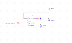
Is there a reason why you would put the series diode in the source leg?
I would tend to put it in the drain leg, where it doesn't influence the gate drive loop.
BTW: Probably you will need a real driver or at least two BJTs to drive the switch.
Is there a reason why you would put the series diode in the source leg?
It's in the drain of a p-MOSFET.
 . But the whole circuit... I don't know what it is supposed to be. Smoke generator?
There is always a chance that the system might be forced out of the soft switching mode. Disturbances, or during start, or with catastrophic input signals, or load dump, or load shorts.
In designs, which would just generate some more heat in this case there would be no reason to add the diodes.
BUT here with these unsaint high voltage devices, such an operating mode has a high chance to become lethal. I would not dare to keep out the diodes in this application.
Diodes:
Is there a reason why you would put the series diode in the source leg?
I would tend to put it in the drain leg, where it doesn't influence the gate drive loop.
BTW: Probably you will need a real driver or at least two BJTs to drive the switch.
The conceptual schematic does not include any details about the actual implementation. Obviously I'm not planning to use an integrated flip-flop. In fact I feel this is going to be the hardest part to design, because even if it has to behave as a conventional S/R, it requires high output current capability and a very well defined 0 to 1 transition voltage at the set input, as the difference between the current leaking trough the diode's parasitic capacitance and the diode forward current is going to be small. Insensitivity to dV/dt and a reasonable speed (I think 250 nanoseconds of propagation delay would be fine, so it needs not be the fastest digital circuit ever) are also a must.
The problem lies not only in the design itself but also in getting it done in a simple, easy to layout way.
To protect against bad loads my idea is to route part of the output current to ground by an inductor. This should make some of the ripple current independent from the load, which is important to avoid excessive ripple voltage at the output, since load capacitance is only an order of magnitude above parasitic capacitance. Protection against shorts is inherent in the circuit (edited: maybe not, but I would implement it in the form of duty cycle limiting and not in the output stage, which I think should be as simple as possible), protection against open circuits would be provided by this inductor, and the flip-flop design warrants the circuit would stall in case of almost any failure condition I can imagine. This would be solved by resetting the circuit, either powering it down or pressing a dedicated button.
A circuit firing one of the flip-flops at startup is needed but it's my least concern right now. The loses during this first shot are going to be big in terms of power but tiny in terms of energy, as the small 50 pF parasitic capacitance needs to be filled to 1kV through the transistors only once.
Last edited:
It's in the drain of a p-MOSFET.
..oohps. p-chanel? - Yes, obviously p-chanel. Sorry, I was blind.
..oohps. p-chanel? - Yes, obviously p-chanel. Sorry, I was blind.
The final design will use n-channel mosfets, but this one is just for testing the concept in spice and a complementary design is easier to debug.
Hm, if we guess that the gnd of the flip flop is connected to the source of the p-chanel, we can be sure that the Mosfet is always OFF.
The output of the flip flop can only deliver gate signals with the polarity which keeps the MosFet OFF. Strange.
Iono:
Nobody except you seems to understand the intension of your circuit.
Any hint?
Don't think of the flip flop as TTL level (0 = 0V 1=+5V) digital device but as one whose output voltages have been choosen so 1 equals the voltage needed to turn on the mosfet and 0 the voltage needed to turn it off. It would be something like 0 = 0V and 1 = -7V. The one and zero voltages at the set pin wouldn't be "TTL standard" either, but this does not make the block stop being a flip-flop.
...still don't get your intension...
What is your plan to do with the clock input?
It would be great if you could describe, which event shall trigger the flip flop to show 1 (MosFet ON), which event shall trigger the flip flop to show 0 (MosFet OFF) and how long these states shall last.
BTW:
Don't kill yourself. Multiple kV are really not a forgiving field of DIY .
- Status
- This old topic is closed. If you want to reopen this topic, contact a moderator using the "Report Post" button.
- Home
- Amplifiers
- Class D
- High voltage, low current output stage for class D amplifier