Solved!
Thanks for the tips and support")
Works great up to 30V supply. Gain is 10x, perfect, as expected.
The output swing almost rail-to-rail. Impressive from a tube amplifier point of view.
The distortion is almost impossible to measure. I use the FFT of a 60 Mhz-1GS/s digital scope and a humble signal generator is not great, whose sine wave 2nd and 3rd harmonics are about at -50 dB from fundamental.
The amplifier (without output stage yet) is outputing just 3 dB more 2nd harmonic, and 0.5 db of third harmonic at full 24V output swing.
Coming from tube amplifiers, where there's no trouble because of the output transformers, I now need to be very carefull with my speakers. I'll first try with a dummy load, of course. But still, being the first time, it is something that intimidates me a little bit.
As a good practice, I suppose I should place the Vbe multiplier on the heatsink along the output devices, right?
Thanks for the tips and support
Works great up to 30V supply. Gain is 10x, perfect, as expected.
The output swing almost rail-to-rail. Impressive from a tube amplifier point of view.
The distortion is almost impossible to measure. I use the FFT of a 60 Mhz-1GS/s digital scope and a humble signal generator is not great, whose sine wave 2nd and 3rd harmonics are about at -50 dB from fundamental.
The amplifier (without output stage yet) is outputing just 3 dB more 2nd harmonic, and 0.5 db of third harmonic at full 24V output swing.
Coming from tube amplifiers, where there's no trouble because of the output transformers, I now need to be very carefull with my speakers. I'll first try with a dummy load, of course. But still, being the first time, it is something that intimidates me a little bit.
As a good practice, I suppose I should place the Vbe multiplier on the heatsink along the output devices, right?
Bob Cordells method (one of them) is to simply replace the feedback resistor with a massive inductor (to block all AC). The lower feedback return is reinstated. Again the results are virtually the same.
The last image shows the OLG for that method.
I really like that method. Does in one step what I do mucking about with voltage sources. Thanks for that Mooly!
I really like that method. Does in one step what I do mucking about with voltage sources. Thanks for that Mooly!
It is a neat method
Solved!
Thanks for the tips and support
Works great up to 30V supply. Gain is 10x, perfect, as expected.
The output swing almost rail-to-rail. Impressive from a tube amplifier point of view.
Right, come on then. What was letting the magic smoke out. Do tell
If you want a really low distortion source then try a CD player with a test disc.
I suspect you may have had a short somewhere?
For OLG estimations I have the "large capacitor" approach but never directly across the feedback resistor. It is essential I think to keep the "grounding" resistor in circuit. Instead I have split the feedback resistor into two and taken the centre tap to ground via a large capacitor. It is not highly accurate as the output load is different but for a low impedance output impedance it makes little difference in most applications.
What is more important is to ensure that the "grounding" resistor is intact because that can reduce the input stage gain; and introduce a phase shift causing potential stability problems, but this may only be significant when using phase lead compensation. Miller compensation tends to be a fail-safe but is not my preferred option.
But the large inductor would be better - except for any potential LF oscillation, which is probably of no consequence.
Although alread clearly off-topic, I'd like to name two general concerns about the OLG based procedure.Instead I have split the feedback resistor into two and taken the centre tap to ground via a large capacitor. It is not highly accurate as the output load is different but for a low impedance output impedance it makes little difference in most applications.
Firstly, as already mentioned, one additionally needs an estimate for the secod term of loop gain, B in post #53.
Secondly, if I understand rigth, you measure the gain from non-inverting input to output. The loop gain contains the gain from inverting input to output. If there are non-symmetries in the differential input stage circuit, this could be another source of inaccuracy.
Altogether I agree that for a simple circuit like the starting one here, the OLG approach is OK.
My method from earlier days was: place an L/C low pass at amp output (large values), place an "AC 1" source between junction of L and C on one side and input of feedback network on the other side, measure voltage at amp output. This leaves intact DC loop and yields loop gain, since the L/C junction is grounded for AC. Loading of amp output is inaccurate with this approach, too. Driving impedance of feedback network is assumed to be zero, although it should be open-loop amp output impedance, which could be larger at higher frequencies.
Now I am completely happy with the methods from LoopGain.asc and LoopGain2.asc; once you used them a couple of times, they are very convenient.
Matthias
Last edited:
Right, come on then. What was letting the magic smoke out. Do tell
Oh, well...
Emitter collector reversed transistors.
I usually double/triple check things, but I was almost absolutely sure that I remembered the pinout of these parts. Of course, I didn't.
A few thoughts about heat...
I designed the amplifier to deliver about 3W to an 8 ohm load, with an input of 0.5Vrms.
But, using 24V DC supply, if the input raises (an it can), the output can swing to around 8.5Vrms (24pk-pk/(2*sqrt(2))).
This is 1.06 Arms or current (OK) but power dissipation on the output transistors would raise to about 25W both (from just a little bit over 3W both, when working at 3W output power).
Should I lower the supply voltage? Is there anything else I can do to limit the output power?
the output transistors work on alternate half waves of the output current. i.e. 50% duty cycle.A few thoughts about heat...
I designed the amplifier to deliver about 3W to an 8 ohm load, with an input of 0.5Vrms.
But, using 24V DC supply, if the input raises (an it can), the output can swing to around 8.5Vrms (24pk-pk/(2*sqrt(2))).
This is 1.06 Arms or current (OK) but power dissipation on the output transistors would raise to about 25W both (from just a little bit over 3W both, when working at 3W output power).
Should I lower the supply voltage? Is there anything else I can do to limit the output power?
The peak current last for a short portion of that halfwave pulse.
You can use the shorter term SOA curves for this duty.
Many power transistors have 150% @ 100ms compared to the DC rating and can go to around 300% @ 10ms. Have a look at your datasheets.
A few thoughts about heat...
Have a read at all this. Maximum heat generation doesn't occur at maximum output.
https://www.updatemydynaco.com/documents/Class_B_Amplifier_Dissipation_Calculations.pdf
Worth reading these two papers from an old electronics magazine.
Bensen did a spread sheet for mosFET output stage based on David Eather's work.
David's temperature de-rated section has a mistake.
The SOA curve goes down in Voltage to reach the new Vce vs Ie.
i.e. the voltages do not change, it's the permitted currents that change, downwards as temperatures rise above Tc=25degreesC.
Attachments
Last edited:
The output transistor dissipation is calculated from Pin-Pout, assuming that these dissipate all of the power (which is close but not quite true). With +/-12V supplies a peak output of 6W (3W rms) requires a peak current of just under 1A - so let's say 1A=8V into 8 ohms =4W rms. The average supply current is 1/pi (look this up if you need to) or 0.318A giving 12*0.318=4W per side=8W total input. That makes the combined output transistor dissipation only 8-4=4W or another way is to see that the amplifier is 50% efficient. But to handle 1A I would still suggest higher power transistors than BD139/BD140, perhaps TIP31/TIP32.
To see what is happening, you can make a spreadsheet of the input and output powers to find the worst case efficiency. But that assumes resistive loads. In practice speakers can be reactive and that causes transistor dissipation to increase. So much for inductors not "consuming power"- they force the transistors to conduct out-of-phase currents which causes their higher dissipation.
To see what is happening, you can make a spreadsheet of the input and output powers to find the worst case efficiency. But that assumes resistive loads. In practice speakers can be reactive and that causes transistor dissipation to increase. So much for inductors not "consuming power"- they force the transistors to conduct out-of-phase currents which causes their higher dissipation.
Last edited:
I just finished building the amp on a protoboard.
It works perfect without the output stage.
But when finished, it oscillates
Without load, the oscillations are quite large.
With load, if I bias the output transistors almost to cut-off, the oscillations are very small.
If I bias for 30 mA idle current, the oscillations grow (not as much as with no load).
The 200 pF Miller cap is in place.
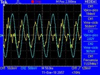
Attached scope captures showing all these oscillations.
It works perfect without the output stage.
But when finished, it oscillates
Without load, the oscillations are quite large.
With load, if I bias the output transistors almost to cut-off, the oscillations are very small.
If I bias for 30 mA idle current, the oscillations grow (not as much as with no load).
The 200 pF Miller cap is in place.
Attached scope captures showing all these oscillations.
Attachments
Another one for tomorrow
Try using jpg or PNG format for the images The BMP just show as downloadable files to me.
Have you got the Zobel network present ?
You could try adding a small cap (say 47pF) across the 9k feedback resistor. See if that helps. Use what you have.
Another thought is that this could be down to layout and grounding.
Try the cap first.
Try using jpg or PNG format for the images
The BMP just show as downloadable files to me.Have you got the Zobel network present ?
You could try adding a small cap (say 47pF) across the 9k feedback resistor. See if that helps. Use what you have.
Another thought is that this could be down to layout and grounding.
Try the cap first.
This oscillation contradicts simulation analysis. In theory, this is rare or impossible.
Do you have the Zobel in place?
From the earlier posts, I see no capacitor across the Vbe multiplier. This is unusual and once resulted in oscillation in a simulation for me, too.
Do you have long leads between reservoir capacitors / power supply and circuit? Or might there even work an interaction between circuit and current-limited supply?
Even if frequency is not too high: you could try base stopper resistors at the output transistors and even drivers.
Good luck,
Matthias
Last edited:
Yes, zobel network in place.
I found something.
- Small cap (~47pF) in parallel with feedback resistor doesn't work.
- Cap in parallel (~47uF) with Vbe multiplier doesn't work.
- Cap in parallel (~1uF) with 220 ohm connecting driver's emitters doesn't work.
- If I open the feedback loop, oscillations persist.
- If I disconnect OTs from circuit, oscillations cease.
- If I connect one of the OTs, oscillations don't come back.
- If I connect BOTH OTs, there're oscillations again.
- If I dicconnect one of OT's emitters, oscillations cease.
- As sson as I reconnect it, there're oscillations again.
Oscillations seem to be around 25 Mhz.
I tried supply voltages 18 ~ 24 Vdc.
All of the above is without feedback (or with feedback; both oscillate)
Removing the OT's emitter resistors has impact, also lowering the supply voltage.
Also, changing the place where I connect the feedback capacitor ground, seems to have impact (though oscillations persist).
After some good hours of test&check, I'm lost at this point.
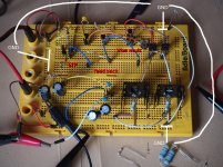
Would a picture of my protoboard help?
Any tip?
Removing the OT's emitter resistors has impact, also lowering the supply voltage.
Also, changing the place where I connect the feedback capacitor ground, seems to have impact (though oscillations persist).
After some good hours of test&check, I'm lost at this point.
Would a picture of my protoboard help?
Any tip?
A picture may help.
This is in some ways a classic symptom of layout and the way various points in the circuit interact.
Not totally relevant perhaps but have a look:
Oscillograms/Testing, and why layout matters.
Does the amp oscillate with nothing connected to the inputs ? and does it oscillate if the input is grounded ?
Have to leave it for now
With the input DC grounded, the oscilations stop (just very very low oscillation at the output).
I tried to remove the input resistor divider and get the +12V from a separate DC regulated supply. Nothing changes.
Also the GND on the protobard does not loop. Three of the rails are connected, but there's no loop. I drawn it on the picture.
Also, when oscillating, the OT that gets warm is the PNP, not the NPN, which remains cold (not even lightly warm).
Attachments
- Status
- This old topic is closed. If you want to reopen this topic, contact a moderator using the "Report Post" button.
- Home
- Amplifiers
- Solid State
- Help with design for a simple low power audio amplifier