Somethings you could try, 100-180 pf and/or twin diodes across LTP collectors, 22-47 pf across B-C of Q7, .047-0.1 uf across C10 and increase VAS/CCS current to 10ma, one at a time. Some of your earlier pics show some rail sticking.
Mad
47pF across LTP collectors: no effect. 47 pF is the max. I could use, because it degrades the phase margin at 1MHz by 20 degrees.
0.047uF across Q10: no effect.
15pF across B-C of Q7: this is the max. I tried because 15pF degrades the phase margin at 1MHz by 15 degrees. I seems to almost eliminate the remaining oscillation, but it also worsens the rail sticking a lot. So I decided not to use it. Caps below 10pF don't have noticeable effect but they still degrade the rail sticking.
The current through Q7 is 1.17ma this won't change because you short R13, what will change is the current gain. If you don't want to try this, then put a scope on the collector of Q7 and drive to clipping, also scope (AC) at the -rail by R19, at clipping.
Mad
Mad
Last edited:
15pF across B-C of Q7: this is the max. I tried because 15pF degrades the phase margin at 1MHz by 15 degrees. I seems to almost eliminate the remaining oscillation, but it also worsens the rail sticking a lot. So I decided not to use it. Caps below 10pF don't have noticeable effect but they still degrade the rail sticking.
That was predictable because it neglects the impact of the Miller capacitance developed by Q7.
At this stage I should mention that capacitance is related to the width of the collector depletion layer which in turn depends on the voltage at the collector.
Accordingly the presence of a collector load will affect the collector voltage.
As mentioned in earlier posts the collector voltage has an inverse relationship with collector to base capacitance.
On this basis, when the collector voltage is highest as it will be under no signal conditions the collector to base capacitance will be at the highest value - this is since the current drawn through R13 will be low and the voltage drop across this will be at the minimum level.
When the signal input increases the voltage drop across R13 caused by the increase in current through the collector load (5.6k) will result in a decrease in the collector voltage. ( This will not be a positive value on a meter but it is still positive in the sense of being less negative than the -ve rail.)
This in turn will reduce the collector to base capacitance value.
As alluded to in my second sentence , a key point in need of expansion is that a decrease in capacitance corresponds to a reduction in the width of the collector depletion layer.
The width of the base is the distance between the collector and emitter depletion layers.
When the collector depletion layer is caused to decrease the width of the base depletion layer will increase.
When the signal is lowered the reverse situation applies and so the base width will be modulated in both directions of voltage swing.
Due to the changes in the respective depletion layer widths involving the collector and base with signal input level, the current gain of Q7 will be modulated by the changing level of collector voltage.
This phenomenon is known as Early effect - you can search the web for more detailed explanations.
Usually Early effect is not too bad however when the collector current is high more Miller capacitance appears at Q7 input.
Unlike a normal Vas Q7 collector has no following stage presenting a load which would reduce the magnification of Miller capacitance.
Taking the figures you give in post 83 there is no problem with a peak current of 1.25 mA but it becomes one when the peak current is 3.25 mA.
I have calculated the value of Miller capacitance generated under these conditions.
As might be expected the levels are in proportion to the peak currents.
The capacitance levels presented to Q7 input I get are 405 pF and 1035 pF assuming a figure of 2pF for KSC1845.
This poses the question if when the gain of Q7 is being modulated due to base width considerations whether a concurrent increase in the capacitance presented across the input is having too much impact on rolling off in the frequency response while also Q7 gain reduction due to base width modulation is another possible influence.
By my calculations a 3.2 mA peak current has the effect of reducing the - 3db point by over 50 % in comparison to a peak current of 1.25 mA.
To deal avoid these possible pitfalls the emitter and collector currents must both be reduced and the collector load impedance similarly reduced by fitting a bypass capacitor in parallel with the selected value for R13 at 5.6k.
The latter point on a bypass was raised by me in posts 58 and 64 among others as well - such being mentioned by John Ellis in post 59 and Mad Inventor in post 91.
So doing will reduce the collector load impedance and reduce the effect the gain towards unity with increasing frequency where Q7 will behave more like an emitter follower than a common emitter amplifier.
To deal avoid these possible pitfalls the emitter and collector currents must both be reduced and the collector load impedance similarly reduced by fitting a bypass capacitor in parallel with the selected value for R13 at 5.6k.
The latter point on a bypass was raised by me in posts 58 and 64 among others as well - such being mentioned by John Ellis in post 59 and Mad Inventor in post 91.
Thank you. The oscillation is only about 1V p-p now with no load or resisitive load and I only have a single oscilloscope probe, so I can't measure relative to the negative rail.
so I had to connect a 15nF capacitive load to the output, which is about the worst case value for this amp and increases the oscillation about 4x, and removed the 4.7pF capacitor from across R16 this further increases the oscillation about 2x. This way I could see a 8x oscillation amplitude and could detect minor changes.
- Decreasing R13 to 2k7 increased the oscillation a little bit.
- A 470pF 2kV unknown dielectric ceramic capacitor across R13 reduced the oscillation somewhat, to about 70-80%.
- A 1nF 50V X7R capacitor across R13 increased the oscillation to about 140-150%.
- When I soldered a simple wire to Q7 collector and touched it with my finger, it significantly reduced the oscillation to about 50%.
So it seems the Q7 collector is indeed a sensitive point but it's not clear to me what to connect here for effective and repeatable results.
Last edited:
x7R chip capacitors have a tendency towards inductive impedance at higher frequencies. I would not recommend them for AC decoupling. I always use silver mica types but these are expensive. Polystyrene types are cheaper and can be as effective in most cases.
Pure capacitive bypass can sometimes act with parasitic impedances to cause oscillation. The usual cure is to include a low value damping resistor. I have not found this necessary in bypassing a load resistor, but you might try e.g. 47 ohms - a value which happens to be near the standard 50 ohm impedance used for many RF circuits which has lower sensitivity than high impedances.
How does the frequency vary with your various investigations?
I didn't check the oscillation frequency when I made these tests a few days ago. I measured it a while back though when I changed the Miller capacitances (and/ or LTP degeneration resistors) to alter the ULGF. The frequency was always around 1MHz, independent of the ULGF.
I want to mention a possible concern if it hasn't been covered, the lack of compensation capacitors on Q6 and Q8 in the PNP current sources. The base resistors may be enough but I would have ~10nF caps on (C-E) Q6 and Q8, otherwise this constant current circuit can oscillate all by itself.
Thank you. The oscillation is only about 1V p-p now with no load or resisitive load and I only have a single oscilloscope probe, so I can't measure relative to the negative rail.
so I had to connect a 15nF capacitive load to the output, which is about the worst case value for this amp and increases the oscillation about 4x, and removed the 4.7pF capacitor from across R16 this further increases the oscillation about 2x. This way I could see a 8x oscillation amplitude and could detect minor changes.
- Decreasing R13 to 2k7 increased the oscillation a little bit.
- A 470pF 2kV unknown dielectric ceramic capacitor across R13 reduced the oscillation somewhat, to about 70-80%.
- A 1nF 50V X7R capacitor across R13 increased the oscillation to about 140-150%.
- When I soldered a simple wire to Q7 collector and touched it with my finger, it significantly reduced the oscillation to about 50%.
So it seems the Q7 collector is indeed a sensitive point but it's not clear to me what to connect here for effective and repeatable results.
What I suggested in regard to a capacitor in parallel was only a first step to show where the focus needed to be.
To continue Q7 is a common emitter amplifier the same as used for a Vas.
To digress a little to explain the distinction between Q7 and a Vas equivalent - the latter is loaded by the output stage which is only a few k Ohms so the collector diffusion capacitance is moderated by the varying collector due the few k Ohms output stage load.
Q7 has a simple resistor collector load in your original setup. There is no mitigation of the amplification of the collector diffusion capacitance by an external series load.
Amplification increases with current by roughly 40 mS per ma and so if you lower the value of the resistor in series with the emitter - the amplification will increase - so a small change in emitter current can have a huge impact.The measure of conductance that is volts per ampere is measured in Siemens where 1S =1A/1V
Adding the 470 pF capacitor across R13 creates a load which increases with frequency lowering Q7 - 3dB point and in the case of 1nF that is a step too far.
The impact of this has to be considered in the light of the former dominant pole effect of Q7 Miller capacitance - by my calculations equivalent to 1nF without 1nF added in parallel with R13.
If the poles are too close in frequency the dominant pole effect will be compromised which is in line with your results.
To change this you have to change the relativity so there is one dominant pole which involves manipulation of the Q7 collector diffusion capacitance so the value of this is reduced.
To do this the values of R14 and R13 need to be increased.
In the case of R14 this is to reduce the emitter current so the corresponding amount of collector current is reduced - this is to reduce the amplification of the diffusion capacitance.
Next the width of the collector diffusion capacitance of Q7 needs to be reduced to the minimum possible in combination with R13.
This is an inverse function of the voltage at Q7 collector and the voltage at the collector needs to be increased.
This will be a negative value with respect to earth with a collector resistor of 5.6k so you would measure what that is with the aim of making this more negative.
You then need a sufficiently large capacitor in parallel with R13 to discharge whatever residue capacitance that may be to earth.
A suggested value I mentioned earlier for R14 was 2.2k. Give that a try and then try increasing R13 in value.
Looking at a simulation of Self's Invariant circuit the peak emitter current for his equivalent to Q7 is about 0.6 mA with 2.2k emitter resistor.
If you want to limit your circuit to 1.25 mA peak collector current where your tests showed the circuit to be stable you might arrange R13 value to be one that sets this as the maximum for all drive levels.
Under static conditions that might be roughly 0.6 mA.
If you want to try this in step values for R14 try 22k for a start keep the 1nF capacitor in parallel during this process.
Try to avoid capacitors like the 4.7pF lead capacitor around R16 or adding any lag capacitors at the output of Q9.
If you still have problems it would be helpful if a simulation of the circuit was made available - I have too many other commitments to be preparing one at present, but I can find the time to look at one.
I want to mention a possible concern if it hasn't been covered, the lack of compensation capacitors on Q6 and Q8 in the PNP current sources. The base resistors may be enough but I would have ~10nF caps on (C-E) Q6 and Q8, otherwise this constant current circuit can oscillate all by itself.
According to Walt Jung stopper resistors of 100R R8 and R18 in the bases of Q5 and Q8 will avoid that risk. I have his article that appeared in AudioXpress which covered the subject of constant current sources and sinks.
clipping behavior with 6Ohm load
(Hi all, I was on holiday but now I'm back.) I have made a 6-Ohm 50W load resistor, because so far I mostly measured with no load or 15nF capacitive load. Although 50W is not enough for the full output voltage of this amp, the resistor can take a few seconds of overload when it's not hot, so I managed to take oscilloscope images.
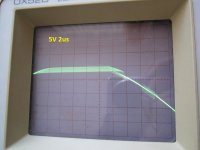
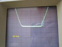
There was no oscillation problem on positive clipping when unloaded or with capacitive loads, but the 6Ohm load brings out that there's oscillation on positive clipping as well, even more severe than on the negative.
The strange thing however that the oscillation with the 6-Ohm load seems to be at much higher frequency, not at 1MHz (which was the case without load or with capacitive loads), but the frequency is now unrecognizeable on my 20MHz oscilloscope. Only an oscillation "fog" can be seen.
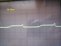
The first image is the positive, second image is the negative clipping with 6Ohm load. third image is an A-B measurement with two oscilloscope probes across the emitter resistor of one of the NPN output transistors. (Regard this A-B measurement only quantitatively, the oscilloscope is not calibrated, and anyway too high common mode voltage was present for this measurement to be accurate.) All images were made with 10kHz heavily clipped sine signal, and Miller capacitance (C5) was changed from 47pF to 33pF for this measurement.
In image 3, it's fairly well visible that when the the amp tries to get away from positive clipping, the current through the output transistor is about doubled for a short time period. This makes my overcurrent protection kick in. So I would like to get rid of this problem if possible.
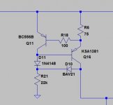
My questions: how would you kill this OPT current increase during the positive rail sticking? I tried to clamp the CCS of the VAS with two diodes, as shown in the fourth image, but it does perfectly NOTHING. I even used two 1N4148 diodes in series to make the clamping effect more pronounced: no use. It seems that it is not the CCS that saturates which is very surprising to me. What else can saturate?
Also, can this very high freq. oscillation occur in the OPS? If so, what could be done?
(Hi all, I was on holiday but now I'm back.) I have made a 6-Ohm 50W load resistor, because so far I mostly measured with no load or 15nF capacitive load. Although 50W is not enough for the full output voltage of this amp, the resistor can take a few seconds of overload when it's not hot, so I managed to take oscilloscope images.
There was no oscillation problem on positive clipping when unloaded or with capacitive loads, but the 6Ohm load brings out that there's oscillation on positive clipping as well, even more severe than on the negative.
The strange thing however that the oscillation with the 6-Ohm load seems to be at much higher frequency, not at 1MHz (which was the case without load or with capacitive loads), but the frequency is now unrecognizeable on my 20MHz oscilloscope. Only an oscillation "fog" can be seen.
The first image is the positive, second image is the negative clipping with 6Ohm load. third image is an A-B measurement with two oscilloscope probes across the emitter resistor of one of the NPN output transistors. (Regard this A-B measurement only quantitatively, the oscilloscope is not calibrated, and anyway too high common mode voltage was present for this measurement to be accurate.) All images were made with 10kHz heavily clipped sine signal, and Miller capacitance (C5) was changed from 47pF to 33pF for this measurement.
In image 3, it's fairly well visible that when the the amp tries to get away from positive clipping, the current through the output transistor is about doubled for a short time period. This makes my overcurrent protection kick in. So I would like to get rid of this problem if possible.
My questions: how would you kill this OPT current increase during the positive rail sticking? I tried to clamp the CCS of the VAS with two diodes, as shown in the fourth image, but it does perfectly NOTHING. I even used two 1N4148 diodes in series to make the clamping effect more pronounced: no use. It seems that it is not the CCS that saturates which is very surprising to me. What else can saturate?
Also, can this very high freq. oscillation occur in the OPS? If so, what could be done?
Attachments
Have you tried increasing the power supply rails to the pre-stages rather than having a voltage drop in the filter sections you originally showed?
Clipping can be caused by voltage or current limiting.
I still have a concern that active current control involves a second transistor that will generate an additional phase shift at some point. As this is a ccs, you could try replacing the BC556 with two 1N4148's just to make it passive and see if that has any improvement.
(Hi all, I was on holiday but now I'm back.) I have made a 6-Ohm 50W load resistor, because so far I mostly measured with no load or 15nF capacitive load. Although 50W is not enough for the full output voltage of this amp, the resistor can take a few seconds of overload when it's not hot, so I managed to take oscilloscope images.
There was no oscillation problem on positive clipping when unloaded or with capacitive loads, but the 6Ohm load brings out that there's oscillation on positive clipping as well, even more severe than on the negative.
The strange thing however that the oscillation with the 6-Ohm load seems to be at much higher frequency, not at 1MHz (which was the case without load or with capacitive loads), but the frequency is now unrecognizeable on my 20MHz oscilloscope. Only an oscillation "fog" can be seen.
The first image is the positive, second image is the negative clipping with 6Ohm load. third image is an A-B measurement with two oscilloscope probes across the emitter resistor of one of the NPN output transistors. (Regard this A-B measurement only quantitatively, the oscilloscope is not calibrated, and anyway too high common mode voltage was present for this measurement to be accurate.) All images were made with 10kHz heavily clipped sine signal, and Miller capacitance (C5) was changed from 47pF to 33pF for this measurement.
In image 3, it's fairly well visible that when the the amp tries to get away from positive clipping, the current through the output transistor is about doubled for a short time period. This makes my overcurrent protection kick in. So I would like to get rid of this problem if possible.
My questions: how would you kill this OPT current increase during the positive rail sticking? I tried to clamp the CCS of the VAS with two diodes, as shown in the fourth image, but it does perfectly NOTHING. I even used two 1N4148 diodes in series to make the clamping effect more pronounced: no use. It seems that it is not the CCS that saturates which is very surprising to me. What else can saturate?
Also, can this very high freq. oscillation occur in the OPS? If so, what could be done?
Consider that a lower impedance will generate a greater feedback signal not only into the divider but also unattenuated via R17 right into the mid point in your low pass filter.
Have you tried increasing the power supply rails to the pre-stages rather than having a voltage drop in the filter sections you originally showed?
Clipping can be caused by voltage or current limiting.
I still have a concern that active current control involves a second transistor that will generate an additional phase shift at some point. As this is a ccs, you could try replacing the BC556 with two 1N4148's just to make it passive and see if that has any improvement.
If the purpose of Q7 and Q9 is to work as a two pole filter and Q7 is a common emitter amplifier capacitance will develop between the base of Q7 because R13 is not bypassed. Accordingly there are two sources of phase shift feeding Q7 - the filter and the impact of Miller capacitance.
One of the impacts of added external Miller capacitance is to split the pole shifting the one higher in frequency making this smaller and making the lower pole dominant.
There is no added collector to base capacitor between collector and base of Q7 but there is a capacitor path from the collector of Q9 to Q7 base.
Q9 phase shifted output will be summed with Q7 Miller capacitance at the signal input point of Q7 base. The latter will be variable and therefore non-linear.
The aim of the structure around Q7 is to develop gain at lower frequency and have this roll off to 1 at a point where the phase shift does not impact on the dominant pole - that has to be through bypassing R13 to zero volts by a suitable value capacitor. In this way a linear capacitor is being used instead of one that varies with Q7 collector voltage.
That's not oscillations on the positive clip. It's just a clip level that follows the power supply ripple. If you adjust the sweep to near 120xN, you will see the clip wave up and down as it beats with the supply ripple frequency, or sync to "line"(AC) and you will just see just one clip line.
That type of constant current circuit should have a ~10n cap across Q11 C;E to stabilize the feedback to Q16. It also improves the collector impedance of Q16 by shunting the Miller capacitance of Q16. R18 is maybe not a great idea. Maybe it's an alternative to the cap on Q11 but not as good. ~R18 plus another resistor Q11 C;B can reduce the minimum voltage drop by say 0.3V, which can be important for low voltage (12VDC) amps, where you struggle to get rail-to-rail output, or you just want to squeeze every watt possible out of your amp. An extra Volt swing can add ~10 Watts to your speakers and off the heat sink.
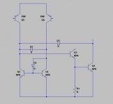
This partial schematic illustrates a way to avoid positive rail sticking. Add a diode D1 to the raise the current mirror base voltage to match the base voltage of Q3. Then put a clamping diode between collectors of the diff amp. So when the diff amp swings too far towards Q6, it shorts out the current mirror and clips before Q4 is completely off.
For this to work, the average voltage on both collectors has to be the same or very close. It also improves the accuracy of the current mirror, which improves the diff-amp and output DC offset.
For this to work, the average voltage on both collectors has to be the same or very close. It also improves the accuracy of the current mirror, which improves the diff-amp and output DC offset.
Attachments
The aim of the structure around Q7 is to develop gain at lower frequency and have this roll off to 1 at a point where the phase shift does not impact on the dominant pole - that has to be through bypassing R13 to zero volts by a suitable value capacitor. In this way a linear capacitor is being used instead of one that varies with Q7 collector voltage.
To get this to work properly the value of R14 needs to be increased to what Self used in his Blameless. He used 2.2k which will reduce both the emitter and collector current levels.
The voltage gain of a common emitter amplifier depends on the current. The value of R13 will need to be increased also to further limit the collector current.
This will make Q7 work more like a buffer and if you get the current down sufficiently to a set level you won't be needing the additional clamp transistor used by Self.
The value of R13 I would suggest - multiples of 10k should be determined more precisely through simulation. Another point about this is you are not only limiting the excursion capability but the working range of Q7.
This may sound to be a silly statement however a transistor is more linear when it is working over a shorter distance on a curve or a line having any slope. It just has to be long enough without going overboard.
- Status
- This old topic is closed. If you want to reopen this topic, contact a moderator using the "Report Post" button.
- Home
- Amplifiers
- Solid State
- Help! Oscillation and "rail override" problem with my power amp