The open loop response
Hello Edmond,
I am looking over the Pheonix circuit modifications and will need a couple of days before I make any comments ( busy with work) .
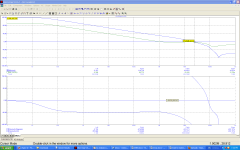
But I have one outstanding question in posting #219 of this thread I attached a file which was my attempt at the open loop gain , using this approach on Pheonix3.cir I get the following Phase margin , which seems a bit confusing. The DB(v(out)) is 21.58MHz at 0 dB which seems a too high, where as DB(V(U,FB)) at 0db is 1MHz PM=85 degrees which seems a bit more like it. Am I looking at this information the right way? is this the open loop response of the amp. I am just curious on how to get the combined loop gain of the whole amp and in fact if this is how to do it.
With regards to the 22R as apposed to the 4R7 (for the base resistors of the output transistors) I have found that 22R eliminates parasitic oscillations which can occur with the Sanken 2SC2922 and 2SA1216 in practice (my experience). Another person who does a similar thing is Bruno Putzey.
Regards
Arthur
Hello Edmond,
I am looking over the Pheonix circuit modifications and will need a couple of days before I make any comments ( busy with work) .
But I have one outstanding question in posting #219 of this thread I attached a file which was my attempt at the open loop gain , using this approach on Pheonix3.cir I get the following Phase margin , which seems a bit confusing. The DB(v(out)) is 21.58MHz at 0 dB which seems a too high, where as DB(V(U,FB)) at 0db is 1MHz PM=85 degrees which seems a bit more like it. Am I looking at this information the right way? is this the open loop response of the amp. I am just curious on how to get the combined loop gain of the whole amp and in fact if this is how to do it.
With regards to the 22R as apposed to the 4R7 (for the base resistors of the output transistors) I have found that 22R eliminates parasitic oscillations which can occur with the Sanken 2SC2922 and 2SA1216 in practice (my experience). Another person who does a similar thing is Bruno Putzey.
Regards
Arthur
Attachments
loops
Hi Arthur,
Although it is the open loop response of the amp, this is not what we are looking for. Admittedly, the terminology is a bit confusing, but 'open loop response' (of an amp) is not the same as 'loop response' (of a loop), that is, the gain and phase response of a specific feedback loop. The latter is roughly equal to the open loop response divided by the closed loop response. But I never use this relationship, as it it prone to errors. I always look at the properties of a specific FB loop itself.
> I am just curious on how to get the combined loop gain of the whole amp and in fact if this is how to do it.
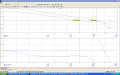
Hmm... difficult question. I don't know the right answer. The problem is that the amp has several separate loops, so how on earth you define the response of the combination of all those loops? For the time being, I think the best you can do is breaking the loop at the point that determines the overall gain of the amp (=closed loop gain). Normally, this is also the most outer loop. In this case between node 'out' and R3. (see & run: pheonix3-outer-loop.cir)
Cheers,
E.
Hello Edmond,
I am looking over the Pheonix circuit modifications and will need a couple of days before I make any comments ( busy with work) .
But I have one outstanding question in posting #219 of this thread I attached a file which was my attempt at the open loop gain , using this approach on Pheonix3.cir I get the following Phase margin, which seems a bit confusing. The DB(v(out)) is 21.58MHz at 0 dB which seems a too high, where as DB(V(U,FB)) at 0db is 1MHz PM=85 degrees which seems a bit more like it. Am I looking at this information the right way? is this the open loop response of the amp.
[snip]
Regards
Arthur
Hi Arthur,
Although it is the open loop response of the amp, this is not what we are looking for. Admittedly, the terminology is a bit confusing, but 'open loop response' (of an amp) is not the same as 'loop response' (of a loop), that is, the gain and phase response of a specific feedback loop. The latter is roughly equal to the open loop response divided by the closed loop response. But I never use this relationship, as it it prone to errors. I always look at the properties of a specific FB loop itself.
> I am just curious on how to get the combined loop gain of the whole amp and in fact if this is how to do it.
Hmm... difficult question. I don't know the right answer. The problem is that the amp has several separate loops, so how on earth you define the response of the combination of all those loops? For the time being, I think the best you can do is breaking the loop at the point that determines the overall gain of the amp (=closed loop gain). Normally, this is also the most outer loop. In this case between node 'out' and R3. (see & run: pheonix3-outer-loop.cir)
Cheers,
E.
Hello people!
I also read the book of Slone and tried to build one of his amps. First I run into problems, but then, by experimentation with different VAS designs I realised that they come from the darlington or beta-enhanced VAS.My solution was to use a Cascode VAS.
Here is my Amplifier: Home - DIY Corner
I also read the book of Slone and tried to build one of his amps. First I run into problems, but then, by experimentation with different VAS designs I realised that they come from the darlington or beta-enhanced VAS.My solution was to use a Cascode VAS.
Here is my Amplifier: Home - DIY Corner
Hi Leon,
Apparently, luck was on your side. The VAS current in your version is also weakly defined (as in the original design), i.e. not rock steady controlled.
edit: If the input stage and current mirrors were perfectly balanced, the output current of the c-mirrors is zero, ergo the standing VAS current is zero as well.
Cheers,
E.
Last edited:
Hi Wahab,
OK. This can be explained by the (nonlinear) loading effect of the drivers.
1. By how much? 1dB or 10...20dB?
2. Due to what? The unloading effect or increased loop gain?
Therefore, may I suggest to use another test circuit, that doesn't suffer from DC drift altogether?
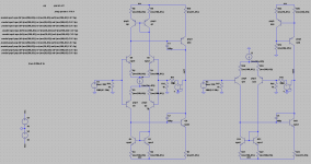
What about this one as shown below? An idealized 'blameless' amp, except the VAS, which is a 'real' tranny. The IPS is a transconductance stage with a gain of 20mA/V and the OPS is a simple voltage follower with a gain of 1. THD20k-TPC = 32.7ppm; THD20k-TMC = 29.5ppm.
Since the effect of TPC vs TMC is only marginal, I think that the slight improvement should only be attributed to the unloading of the VAS. If the VAS has benefited from TMC to the same extent as the OPS, then the improvement should be much higher, in the order of 10...20dB, which is not the case.
Cheers,
E.
Hi , Edmond
A few datas about the subject...
Vas loading seems not to be the main culprit..
I kept the same circuits to sim the following parameters.
The VAS is loaded by a triple EF to keep its loading at
minimal value.
As shown by the curves, the OLG deacrease very little
when the output stage is loaded , thus, the VAS loading
is no more the dominant source of THD in that circuit..
The rising THD is due to the OPS varying gm(s) , as shown
by the THD ratio deacreasing when IQ is badly increased, thus
reducing the relative gm(s) variation in respect of the output
level...
The available NFB provided by TMC from 20khz to
200khz is about 20db, while the loaded OPS THD
increasement is on the same order at 20khz and
soaring with fequency increasing.
cheers,
w
Attachments
Apparently, luck was on your side. The VAS current in your version is also weakly defined (as in the original design), i.e. not rock steady controlled.
Well, I must admit that this balancing issue with the input stage is very strange thing, but it was not luck that I made it working.Luck can be by one amplifier, but not by two or three.And in fact I had some luck with the first amp, at that time I only wanted to fix the ocsilations problems.And I still don't understand how it can oscillate without an input signal, but it only happens with darlington VAS.The only thing wich remains not very good is that the bias voltage for the VAS is not stable, but I don't know how to fix it.But otherwise it works very good.
[snip]
The only thing wich remains not very good is that the bias voltage for the VAS is not stable,
Hi Leon,
That's precisely what I mean: not stable.
but I don't know how to fix it.
[snip]
I've put several examples (a CMCL) on this thread. Another solution is by JCX: http://www.diyaudio.com/forums/solid-state/56860-optoisolator-vas-bias-comp-diff.html#post637347
See also Andy_C about this issue: http://www.diyaudio.com/forums/solid-state/16796-unstable-vas-current-amp-slone-book.html#post195526
Cheers,
E.
Hi , Edmond
A few data about the subject...
Vas loading seems not to be the main culprit..
I kept the same circuits to sim the following parameters. The VAS is loaded by a triple EF to keep its loading at minimal value. As shown by the curves, the OLG decrease very little when the output stage is loaded , thus, the VAS loading is no more the dominant source of THD in that circuit..
The rising THD is due to the OPS varying gm(s) , as shown by the THD ratio decreasing when IQ is badly increased, thus reducing the relative gm(s) variation in respect of the output level...
The available NFB provided by TMC from 20khz to 200khz is about 20db, while the loaded OPS THD increase is on the same order at 20khz and soaring with frequency increasing.
cheers,
w
Hi Wahab,
I agree with all above points, but what about our disagreement whether (and to what extent) the VAS benefits from TMC?
Cheers,
E.
Hi Wahab,
I agree with all above points, but what about our disagreement whether (and to what extent) the VAS benefits from TMC?
Cheers,
E.
Hi, Edmond
Well, i ve got an idea , but still no technical ground
to back it..
TMC is definitely more complex than its aparently simple
implementaton..
Since the VAS is included in the TMC NFBL , we can safely
assume that its eventual THD is reduced as well by the said
compensation/NFBL , but only within some limits :
If the (OPS THD)/(VAS THD) ratio is equal or higher than
the available NFB ratio , all TMC can do is to reduce the
total THD to value at best equal to the OL single VAS.
Perhaps your question is rather whether the VAS
intrinsical THD is also reduced in the VAS + OPS configuration
when TMC is implemented?
This has no object, as with TMC , as with any NFB network , it can occur
that the VAS must produce more THD/error signal to balance the THD
of the output stage.
cheers,
w
The current is not stable because the bias volage is not stable.But why is it not stable? In simulation you have always stable voltage and current for the VAS.So it must be a problem with transistors and not with design.And it's possible to make it working, but you must use good parts.Close matched transistors and resistors.
Hi, Edmond
If the (OPS THD)/(VAS THD) ratio is equal or higher than
the available NFB ratio , all TMC can do is to reduce the
total THD to value at best equal to the OL single VAS.
w
Should read :
all TMC can do is to reduce the
total THD to value at best equal to the OL single VAS THD.
no!it must be a problem with transistors and not with design.
Slone's design is flawed.
There is some speculation in this Forum that he never built this design to find the flaw in it's design.
And yet he built a reputation as an amplifier designer and author and still recommends a flawed amp design!
Last edited:
The current is not stable because the bias volage is not stable.But why is it not stable? In simulation you have always stable voltage and current for the VAS.So it must be a problem with transistors and not with design.And it's possible to make it working, but you must use good parts.Close matched transistors and resistors.
It doesn t work because the current mirrors transistors
drop voltages are lower than the necessary threshold to
make the two VAS darlingtons conduct..
The DC loop will try to balance the whole amp,
but unfortunately, it will do so abruptly , generally by oscillating.
Using a single device as VAS doesn t fit either, as the
current mirrors device are almost saturated and therefore
the once necessary threshold is reached only thanks to
devices dispersion, i.e, if the saturation voltage of the mirrors
transistors is higher than the said single VAS Vbe. Very unlikely..
Implementing resistors in the mirrors emitters help a little,
but a better solution is to put some voltage drop in serial with
the mirrors collectors, using diodes and other similar devices..
This, of course, doesn resolves other important issues
that are equally mandatory to clean up to make the
amp reliably reproducible..
Last edited:
O.K that's your opinion, that this design is flawed, but it works in simulation and even in real life.I've build this amp, so I know what I'm talking about.Even if there are some problems with unstable voltage, it's not that big problem and I think it's due bad transistors.
Leon,
Believe me, read this thread and you will be convinced it is futile to continue with that schematic. I already lost over 1000€ and it still is unstable. Do me a favor. In your amp or in the simulator. Change just the left upper emitter resistor by 1% up or down. Tell me how the VAS standing current behaves?
In my case (that is with Darlington) it varies from 0 mA to 300mA whereas it is 40mA in the simulation if both emitter resisters are identical.
One day it worked in real life with a standing current of 60mA (a bit high but it could work for some minutes). I did the same test raising 1 resistor +1% -> current goes to frying mode -1% -> current goes to zero (or class C operation)
I took pictures an dposted them here.
Go for the CMCL solution Edmond is talking about ...
As for the oscillations with beta enhancers I believe there is argument that without them the current drawn from the IS by the VAS Iq is higher. Namely VAS IQ / HFE
If darlingtons are used that current is VAS IQ / HFE * HFE so to speak. This is said to load the IPS insufficiently.
If beta enhancers are not used the load on the IPS might be just enough.
Please read the start of the this topic ...
Best Regards
Olivier
Slone's design is extremely sensitive to component tolerances. Normally, we call this bad practice.
Yeah, Monte Carlo analysis easily confirm this.
Attachments
Believe me, read this thread and you will be convinced it is futile to continue with that schematic.
Then we should consider all designs with current mirrors futile, but Sony for instance has build a million amplifiers wich have current mirrors and cascode VAS, but are not simmetric and all they work very good.
And there are users here wich have build this amplifier on stripboard and it worked.So it's apparently not bad design (if you are lucky enough).
Last edited:
this is a wrong conclusion.Then we should consider all designs with current mirrors futile,
Slone's design using dual complementary mirrors is flawed.
Most mirrors have been tested by the designer.
- Status
- This old topic is closed. If you want to reopen this topic, contact a moderator using the "Report Post" button.
- Home
- Amplifiers
- Solid State
- HEEEELLLPPP : M. Randy Slone Mirror Image Topology Construction - Troubles