Hi,
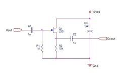
With the help of ChatGPT I was trying to build the minimal JFET buffer.
The requirement for the buffer is to take high impedance preamp output and help to drive low impedance next stage.
So, ChatGPT has suggested the following circuit, claiming «the buffer will effectively isolate the preamp from the lower impedance load that follows».

I am not a real electrical engineer and the circuit kinda makes sense to me. I have tried to assemble it and I get completely no sound at the output. JFET doesn't seem to conduct any signal. I have tried it with J201 and with MPF102, no luck with both.
It is simple enough and I seem to have checked everything multiple times. And ChatGPT keeps insisting it should work and I am stupid.
Could somebody give me a hint? Is it a viable circuit? What is missing for it to work as intended?
Thanks.
With the help of ChatGPT I was trying to build the minimal JFET buffer.
The requirement for the buffer is to take high impedance preamp output and help to drive low impedance next stage.
So, ChatGPT has suggested the following circuit, claiming «the buffer will effectively isolate the preamp from the lower impedance load that follows».
I am not a real electrical engineer and the circuit kinda makes sense to me. I have tried to assemble it and I get completely no sound at the output. JFET doesn't seem to conduct any signal. I have tried it with J201 and with MPF102, no luck with both.
It is simple enough and I seem to have checked everything multiple times. And ChatGPT keeps insisting it should work and I am stupid.
Could somebody give me a hint? Is it a viable circuit? What is missing for it to work as intended?
Thanks.
hoho,
Did you by chance save a transcript of your conversation with ChatGPT? If so, could you please post it here?
You see, something is very wrong and it doesn't seem the usual sort of thing ChatGPT would do most of the time, unless perhaps you made some kind of malformed request?
The circuit you posted cannot work because it violates the very basic need of a transistor to operate with correct CD bias. In the circuit shown there is not correct DC bias.
So, what exactly happened? What exactly did you say to ChatGPT? Then what exactly did it say? I ask for exact wording because computers can sometimes take words literally and so the explanation may be in the choice of wording.
Also, would you explain why you want the most minimal buffer, rather than a very simple yet good buffer?
Thanks,
Mark
Thanks for the responses!
It was a relatively long conversation. I've told it that on my preamp output I have a voltage divider with 220k+10k resistors. I was asking about impedance matching, that I have a 12ax7 preamp which is being sent to the sound card line input. It has suggested that a buffer might be the best choice. I just wanted something quick to validate the idea with the components I currently have in my drawer (I had a few JFETs) before going for a proper solution. So I'll try to paste the relevant part (the entire conversation is too long):

Then (when nothing worked), it was a lengthy troubleshooting conversation. I have even uploaded the schematics I have in the first post to double-check I have got it correctly. But it has lead nowhere. It was refusing to accept that the circuit is wrong, it was telling me to check if the components have proper values and aren't faulty, and so on. In the end it has suggested me to seek help of a qualified person") .
.
It was a relatively long conversation. I've told it that on my preamp output I have a voltage divider with 220k+10k resistors. I was asking about impedance matching, that I have a 12ax7 preamp which is being sent to the sound card line input. It has suggested that a buffer might be the best choice. I just wanted something quick to validate the idea with the components I currently have in my drawer (I had a few JFETs) before going for a proper solution. So I'll try to paste the relevant part (the entire conversation is too long):
Then (when nothing worked), it was a lengthy troubleshooting conversation. I have even uploaded the schematics I have in the first post to double-check I have got it correctly. But it has lead nowhere. It was refusing to accept that the circuit is wrong, it was telling me to check if the components have proper values and aren't faulty, and so on. In the end it has suggested me to seek help of a qualified person
.By the way, I've found a faster way to try the buffer — I've realized that I have Wampler Tumnus pedal which has always on buffer, so I've just tried to put it between the preamp and the sound card and it indeed gives a much better sound.
Out of the buffers from here https://www.muzique.com/lab/buffers.htm — which one would be the best between a 12ax7 preamp output and a sound card line input?
Thanks.
Out of the buffers from here https://www.muzique.com/lab/buffers.htm — which one would be the best between a 12ax7 preamp output and a sound card line input?
Thanks.
Guitar pickups can sometimes put out as much as 2vrms. Anyway, there are lots of jfet buffer circuits for guitar:
https://www.google.com/search?q=sim...1658&prmd=isvnbmtz&rlz=1C1RXQR_enUS1091US1091
https://www.google.com/search?q=sim...1658&prmd=isvnbmtz&rlz=1C1RXQR_enUS1091US1091
The value of the source resister determines the actual setpoint of the J-fet. This 10k may be to high if the Idss is high: the setpoint is lifted above the optimum around 4Vdc and clipping occurs if the input signal nears the supply. It can be to low if the Idss is low: the opposite occurs with ground clipping.It also seems to clip the signal when I hit the guitar harder.
Take that battery and measure the Idss: drain to the plus, gate & source TOGETHER to the minus... and a DMM multimeter in series in the mA range.
Id opt = 9/16 * Idss ( [1 - 1/4]^2 ) = 0.5625 for minimum distortion and maximum signal level (some say 0.7*Idss, but that's to high really).
So, with a unknown Vgs at the optimum Id ("Vgsopt≈Vpo-median), one can estimate the resistor at { (Vsupply / 2) - 0.7 } / { 0.56 * Idss-measured}.
J201 (#7):
Idss minimum = 0.20mA -> Rs = { (9/2) - 0.7 } / { 0.56 * 0.2 } = 3.8 / 0.112 = 33k93 (33k0)
Idss median = 0.45mA -> Rs = { (9/2) - 0.7 } / { 0.56 * 0.45 } = 3.8 / 0.252 = 15k08 (15k0)
Idss high = 0.70mA-> Rs = { (9/2) - 0.7 } / { 0.56 * 0.70 } = 3.8 / 0.392 = 9k694 (10k0)
Idss maximum = 1.00mA-> Rs = { (9/2) - 0.7 } / { 0.56 * 1.00 } = 3.8 / 0.56 = 6k786 (6k8)
In general, the value of 10k is not always the best value, and clipping can occur.
Take a 6k8 resistor in series with a 10k log (B) variable resistor - adjust for lowest distortion.
Calculations in 10 minutes, typing 20 takes minutes (also foc).
Everything is logarithmic, except human perception AI is a human child.
Hit the wall: the gate needs a bias halfway the supply!
The above is only valid with an extra resistor from the supply to the gate, also 1M, lifting the gate to 1/2 * the Vsupply.
Do Androids Dream of Electric Sheep?
The above is only valid with an extra resistor from the supply to the gate, also 1M, lifting the gate to 1/2 * the Vsupply.
Do Androids Dream of Electric Sheep?
I know the solution to the problem has been mostly found, but circling back to what's wrong with the AI buffer:
1. As @Markw4 said, there's no DC bias or reference for the source.
2. Even if there were, at AC, the output is connected via low impedance to ground through the 10uf cap. JFET source output impedance equals 1/gm [gm=transconductance=yfs=gfs]. This forms a voltage divider with the capacitor, creating a low pass filter. If we use 2mS as our gm, that's 500 ohms, and the -3dB point is 32hz, so at 320hz your output is 23dB down and at 3.2k it's 43dB down.
BTW, J201 has a breakdown voltage of 40V, higher than most opamps. Replace 9 with whatever voltage you want in all of @Citizen124032's design equations and you will gain headroom.
Last edited:
ChatGPT is completely unsuitable to solve any engineering problems, by sheer design.And ChatGPT keeps insisting it should work and I am stupid.
It basically just parrots what it found on the internet or whatever one used to "train" it, and stages things so that its output looks somewhat plausible.
Just noticed, @Citizen124032 , I think the -.7V in your equations should be +.7V, right?

Vpo should be mostly irrelevant for a source follower, and higher Vpo leads to higher likelihood of clipping if gate bias is mid-supply. Gm is the important spec. Ignoring bias voltage and transistor non-linearity, the follower circuit is a voltage divider with Vout=Vin*(RL/(RL+[1/gm]); RL is parallel combination of bias impedance and load impedance. Less voltage drop across the non-linear transistor results in less distortion. See sim results below, where THD scales with 1/gm (Qspice sim file also attached). Higher Vpo (=higher Idss) JFE202 performs worse at same bias current because gm is slightly lower at that current. No output voltage clipping on any of them.If you want enough headroom, don't use a j201 in this circuit. It has a low Vgs and will clip already with a low signal level. Use a Jfet with a bigger Vgs value like J112. I wonder what the chatbot would suggest as a suitable Jfet for a buffer and why.
Attachments
The difference between a sign and an equation: +a - -b = +a + b. It's tricky indeed, but the formulas are ok of this spacing is followed.Just noticed, @Citizen124032 , I think the -.7V in your equations should be +.7V, right?
So, the - .7V should be read as - ... +0.7V proper.
I've written down uncountable paper pages of equations with these +/- errors, to take abundant space between those signs. The stacks are good to heat the house for centuries...
Be critical, a review will be well appreciated! I'll work it over again if needed whatsoever.
3.8V at source with gate at mid-supply gives a .7V forward bias on the gate...J201 (#7):
Idss minimum = 0.20mA -> Rs = { (9/2) - 0.7 } / { 0.56 * 0.2 } = 3.8 / 0.112 = 33k93 (33k0)
Idss median = 0.45mA -> Rs = { (9/2) - 0.7 } / { 0.56 * 0.45 } = 3.8 / 0.252 = 15k08 (15k0)
Idss high = 0.70mA-> Rs = { (9/2) - 0.7 } / { 0.56 * 0.70 } = 3.8 / 0.392 = 9k694 (10k0)
Idss maximum = 1.00mA-> Rs = { (9/2) - 0.7 } / { 0.56 * 1.00 } = 3.8 / 0.56 = 6k786 (6k8)
Also in my above post JFE202 should read JF202. And additional note, all models were the Linear Systems manufacturer-provided (I think) models included with Qspice.
- Home
- Source & Line
- Analog Line Level
- Having fun with JFET buffer and ChatGPT...