We are both referring to nested loops. There is one forward path through the integrators, but n feedback paths.mikeks said:
I am not certain i understand....'minor-loop' and 'outer loop' may be the source of confusion here.....they do not mean the same thing.....
Nevertheless, if you mean output stage distortion is still the limiting factor, even with the output stage enclosed within the compensation loop, then i agree...
This means each loop is closed (typically at unity gain) and the next one built around this. I'm not familiar with the academic terminology but from your post I gather all the loops "inside" the final loop are called "minor" loops. I call the biggest loop the "outer loop", and I have no idea if it would otherwise be called the "major" loop. I've never seen the insides of a university, so bear with me if I get the official terminology wrong.
")
One can build an op amp in this manner, because the dominant pole is that of the outer loop. Increasing closed-loop gain increases phase margin.
As for the output stage's errors, they see the compound loop gain of all the loops around it. Its contribution to THD is readily made negligible.
On the other hand, the nonlinearity of the first integrator (the one which forms the outer loop cq the dominant pole) is not reduced by the other loops. Its output carries the whole signal. This is what I mean by saying that the distortion from the output stage is quite readily taken out of the equation, but that of the (miller or other kind) VAS remains. Granted it's easy to get that down quite easily to 10ppm, but not to 0.1ppm.
I believe this is what JohnW is alluding to as the first integrator being the final determining factor in linearity.
An n-th order loop can also be formulated in the converse way, with a single feedback path but with n feedforward paths. You make a cascade of integrators and derive the output from a weighted sum of all integrations. This is how noise shapers are typically constructed.
Only the output of the last integrator actually carries the signal. The one-before-the-last carries the derivative of the output signal and so on until the first integrator that hardly moves at the output. If the output of the first integrator carries pretty much no signal, its linearity becomes uncritical.
This construction is the fastest route to ridiculously low distortion figures. Unfortunately it can only be used with a fixed gain. As said, no problem for buffers and power amps, but rather useless when you're trying to make an EQ.
You have my sincerest sympathy. I've had similar setbacks over the years.JohnW said:
I’m having a SMALL personal crisis, I just directly compared a NEW DAC design which is the indirect result of say 10 years of work, 127dB dynamic range, THD 0.000028% FS etc – and compared it to a CD player I designed back in 1995 (had the unit back to repair for a friend) – the difference is enormous - I mean HUGE – the 1995 design is way better!
So PMD100 and SAA7350 on steroids (external I-V and VRef circuits) beats DAC with 32Bit internal data path – 4th order noise shaper with Quad array 128 level PWM output, 512 tap length digital filter, sub 3pS clock jitter
A few remarks. 32 bits seem quite low for a serious noise shaper. I have a fairly simple 6th order 1-bit noise shaper in my DAC and the word length ended up at 36 bits. I don't know what the internal sample rate of your noise shaper should be, but if the PWM is inside the loop, prepare for huge word lengths.
Another thing not to forget is proper dither.
You are quoting 3ps. What is 3ps? cycle to cycle? Over 100k cycles? A 3ps cycle to cycle jitter figure on a 49MHz clock can hide an enormous LF jitter problem. You may have shot yourself in the foot by taking a too high clock frequency.
Cheers,
Bruno
Hi Bruno,
Not wishing to take this thread off the subject too far: -
This is the method I use to construct my integrator loops, but the first integrator input stage receives the input signal and feedback, its input stage is effectively outside the feedback loop. Typically, I’m limited to –120dB to –125dB THD due to “input stage deficiencies”. Of course, the input signal and feedback is “Summed” via resistors, but I find that the common-mode isolation between the integrators input terminals limits the ultimate performance. That’s why I’m sure you also have seen typically –120dB THD with your ADC input stages – try just adding less then 1pF on the inputs of your 1st integrator and watch the THD change – time for small Cap. Trimmers on those inputs
I find that the first and last integrators are the only ones in the chain that have any recognisable signal at their outputs… I wonder why you don’t see a signal on the output of your first integrator – do you have an integrator cap across the first integrator – or rely on the “overall loop” if you see what I mean?
3pS pk-pk over a one second period, the narrowest internal data path being 32 bits, the noise shapers operating with a 48 bit Data path (2x 24 bits). MCLK is 768Fs, but operating on both edges – but yes there’s known problems with internal dithering and “phase modulation” between outputs – seems it was not a good idea to clock on both edges.
Maybe we should start a new thread…?
John
Not wishing to take this thread off the subject too far: -
An n-th order loop can also be formulated in the converse way, with a single feedback path but with n feedforward paths. You make a cascade of integrators and derive the output from a weighted sum of all integrations. This is how noise shapers are typically constructed.
This is the method I use to construct my integrator loops, but the first integrator input stage receives the input signal and feedback, its input stage is effectively outside the feedback loop. Typically, I’m limited to –120dB to –125dB THD due to “input stage deficiencies”. Of course, the input signal and feedback is “Summed” via resistors, but I find that the common-mode isolation between the integrators input terminals limits the ultimate performance. That’s why I’m sure you also have seen typically –120dB THD with your ADC input stages – try just adding less then 1pF on the inputs of your 1st integrator and watch the THD change – time for small Cap. Trimmers on those inputs
Only the output of the last integrator actually carries the signal. The one-before-the-last carries the derivative of the output signal and so on until the first integrator that hardly moves at the output. If the output of the first integrator carries pretty much no signal, its linearity becomes uncritical.
I find that the first and last integrators are the only ones in the chain that have any recognisable signal at their outputs… I wonder why you don’t see a signal on the output of your first integrator – do you have an integrator cap across the first integrator – or rely on the “overall loop” if you see what I mean?
3pS pk-pk over a one second period, the narrowest internal data path being 32 bits, the noise shapers operating with a 48 bit Data path (2x 24 bits). MCLK is 768Fs, but operating on both edges – but yes there’s known problems with internal dithering and “phase modulation” between outputs – seems it was not a good idea to clock on both edges.
Maybe we should start a new thread…?
John
JohnW said:This is the method I use to construct my integrator loops, but the first integrator input stage receives the input signal and feedback, its input stage is effectively outside the feedback loop. Typically, I’m limited to –120dB to –125dB THD due to “input stage deficiencies”. Of course, the input signal and feedback is “Summed” via resistors, but I find that the common-mode isolation between the integrators input terminals limits the ultimate performance. That’s why I’m sure you also have seen typically –120dB THD with your ADC input stages – try just adding less then 1pF on the inputs of your 1st integrator and watch the THD change – time for small Cap. Trimmers on those inputs
I find that the first and last integrators are the only ones in the chain that have any recognisable signal at their outputs… I wonder why you don’t see a signal on the output of your first integrator – do you have an integrator cap across the first integrator – or rely on the “overall loop” if you see what I mean?
I'll just respond to the things that conceivably belong to this thread
)I know your input stage is outside the loop. I was suggesting simply building an input buffer comprising a higher order loop to get rid of its own distortion, separately from the class D power stage which takes care of itself.
When I said the first integrator carried no signal I mean "wanted signal". Of course, in an ADC or class D control loop it carries outband noise.
In the case of a non-quantised, non-sampling system like a linear amplifier (what this thread is about), you'd find not much there.
MikeB said:
Hi thanh !
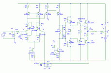
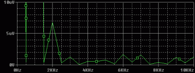
Try cfp'd inputstage with cascoded vas, this can give ~4uv 2nd,2uv 3rd !
Yes ! I have finished building it. And which VAS stage should i use? But in the sim ,my amp still isn't as good as your
I am using 2sc2383/2sa1013 + 2sa1227/2sc2987With tripledarlington output using mje15030/15031+mjl1302a/mjl3281
this is my troubleI think you can get better result with even faster output-bjts.
But i believe you don't need these low thd values, i prefer bandwidthand reliability.
Can current mirror works? I never building asymetrical amp with current mirror.You can get even lower values, i've built one. It was asymetrical,
using jfet+cfp+currentmirror. OL-gain was > 1:1.000.000. It did
not oscillate, but would need shielding as it revealed any electrical
disturbance somewhere in the house. At these ratios, receiving a
single uV from the air can give a well audible peak at the output.
I had some fun with a lightning still far away !
And it didn't sound better than my actual amp.
How can I?Don't forget: If you are simulating, take the time to slightly modify
some Vbe's of transistors to simulate thermal drift.
Are these better than mine?Forgot: You can buy these ! Get some pioneer/yamaha/sony chipamp,
they tend to have that low thd-numbers... (good for marketing)
Don't forget: less gain -> higher bandwidth
He, Mike, you got one good answer with that !Any other answer from the sound quality point of view?
hi lumanauw !
Hmm, no further real answer yet... I now believe that the high bandwidth
is necessary to move some problems from feedback to some frequency
that is no longer audible ?
Ah, one more: avoid to big global FB-loop ?
to thanh:
Yes, it's possible to build amps with that low thd, but only for lower
freqs. These amps are crap for higher freqs...
Don't say that an amp is good because of some low numbers !
If you don't hear any distortions, the thd is low enough...
For asymetrical design (single diffamp) the currentmirror is a very
easy thing. No big biasing and calculating. Just place it on top of
the diffamp. Then feed this into a vas with a ccs on the other side...
For changing vbe, select the transistor, click Edit/model, say "edit instance model",
confirm some alerts, the first entry IS is for the vbe.
Mike
hi lumanauw !
It's both of it, "looking" symetrical and beeing symetrical, and reducing
the gain to get better linearity. The gain of this circuit is already about
1:3.000.000, even more can get dangerous.
The other problem is, that the "min-voltage" the current mirror can supply
is Vce-sat of the bjt + the voltagedrop on the 100ohms. So moving
the bias down gives more ability to swing before the diffamp clips.
In theory...
Yes, but you are right, it would work without r3. Hmm, without r3
i could use a cfp in the vas, maybe boosting the gain to 1:10.000.000 ?
This should give a nice radiotransmitter. Maybe we can start a contest,
who makes the amp with the highest OL-gain... (Stable of course)
Mike
Mike! Thanks you very much!You are kind-hearted and fervous.
Can you pickup a version which uses a cfb in the vas?Thank you!i could use a cfp in the vas
I think an amp is good because of several number and personal hobbyDon't say that an amp is good because of some low numbers !
http://sound.westhost.com/amp-sound.htm
SAA 7350
John,
even if this is off topic: I am surprised you had such nice results with the 7350.
I have a Philips CD-930, with NPX58xx digital filter, Tent clock and lots of supply and reference decoupling on the SAA 7350. Still, it is no match to the AD1854-based DAC with onboard ECL clock that I have slaved a cheapo Kenwood to.
I gather the progress with modern "multilevel" DACs is that the use an array of 1bit sources which are randomly combined and give much better analog performance than a single 1 bit source which is limited by capacitor and transistor nonlinearity, no matter how good the digital processing is.
You might take the SAA7350 further by using a TDA1547 as a dedicated output device, but it's still 1 bit only.
lumanauw said:Hi, Mike,
What is the approximation of this amp's OL gain? It doesnt use RE in VAS, but use R for CCS (does this makes the gain lower compared to using CCS?)
Okay, did some simus on the circuit...
OL-Gain is ~1:50000, OL-Bandwidth is ~100hz (-1db) THD ~0.2%
You really shouldn't look at any numbers on this circuit, i think the
trick was to make an amp violating anything D.Self said...
Maybe it distorts simply in a way sounding good ?
The vas has still big gain, due to miller-cap (the 100uf)
Mike
Hi, Mike,
So it is true, R loading gives lower gain than CCS?
Got an old secret here. R loading maybe looks "Ancient Aged", propably you wont even try. It has 2 here, one in the differential, and the other one is in VAS, with cap in the middle of 2 R.
But I can tell you, it do sounds better than CCS. Try it.
Maybe it is not so good in SIM or electronic theory or electronic measurement, but it really sounded better. Using R certainly generates more THD than CCS, but maybe it is the bigger THD that makes the sound more welcomed to ear. (but not the odd harmonic offcourse)
So it is true, R loading gives lower gain than CCS?
Got an old secret here.
R loading maybe looks "Ancient Aged", propably you wont even try. It has 2 here, one in the differential, and the other one is in VAS, with cap in the middle of 2 R. But I can tell you, it do sounds better than CCS. Try it.
Maybe it is not so good in SIM or electronic theory or electronic measurement, but it really sounded better. Using R certainly generates more THD than CCS, but maybe it is the bigger THD that makes the sound more welcomed to ear. (but not the odd harmonic offcourse)
Hi lumanauw !
In sims it's obvious that the simple r-loading vas is more robust.
It does not need a predriver at all, it does make no difference.
The ccs-style is lost without predriver, it really doesn't like loads.
For this kind of vas, the cfp does a great job again.
I prefer the ccs-style, as it is more steady, you have always the
same current, not changing with supplyvoltage or voltageswing.
This of course is from a technical point of view, not audiophile.
This means, if you just want a steady and reliable amp, the
currentmirrors seems to be the better choice.
I made some test with the r3 (the 330ohm one), the result with r3
are slightly better than without. Much less DC and less harmonics.
The aksa-circuit you posted is obviously designed to distort, with
minimal changes the thd of this circuit can be reduced about factor 30.
(balancing the diffamp and adding a buffer between vas and diffamp, and balancing the feedback)
Mike
another thing...
I start believing, that the impact of harmonics to the sound is completely
overestimated, as long as you don't generate large odd harmonics
by crossoverdistortion or else, everything is fine. The real character
seems to be generated somewhere else. Don't forget, loudspeakers
have harmonics well above 1%, but these are generated in a natural
way, it's still mechanics like instruments...
So with high thd i have 1.2%, with very low thd i have 1.002% ?
So high OL-gain is mainly good for reducing outputimpedance ?
Mike
Hi, Mike,
I'm not talking from the electronic/calculation point of view. Since it is a very simple experiment, changing CCS with single R, maybe you can just try it (Just a little calculation for the value of R). It gives interesting result.
I still cannot figure out how to make 2 CFP to become current mirror. Can you suggest anything?
- Status
- This old topic is closed. If you want to reopen this topic, contact a moderator using the "Report Post" button.
- Home
- Amplifiers
- Solid State
- Have you ever succeed in buiding a input stage with current mirror?