I've update my website with a paragraph on:
OMC versus TPC versus TMC and
How to get rid of the cons and keep the pros of both techniques
I love this one:
website said:For the same reason THD20k is much lower with TMC: 51ppb, leaving TPC in the dust with an embarrassing 1.3ppm.
51 parts per billion vs. 1.3 parts per million, this is SO embarrasing it makes me blush

2. To compensate the main compensation loop of IIC, Bob Cordell notes (p177) that it may be possible to have nested Miller compensation on the (so called) VAS. This is attractive in theory, since it should provide similar benefits as ordinary Miller compensation over shunt compensation. However in his own benchmark amp he does not use this method or the PLIL across the inputs of the SuperTIS, but a series RC across the LTP collectors. Any comments on the 3 choices?
Best wishes
David
Hi David,
Thanks for pointing out the post involved. That is an interesting point you make. At the time I did my MOSFET power amplifier with error correction I probably just didn't think of trying Miller compensation for the local loop formed by the Miller Input Compensation. My main focus at the time was on the two benefits of MIC, namely greatly increased slew rate and a compensation scheme that had both ends of the compensation capacitor referenced to ground, rather than one to ground and the other to a rail.
Also, because the circuit nodes are balanced at the location between the input stage and the VAS, it seemed more straightforward and appropriate to use a differential R-C shunt to achieve the inner loop compensation. I also felt this was OK because the unity gain frequency of the inner loop can be much higher than that of the global loop, so its effect would be less intrusive anyway.
I agree with your concerns about re-introducing the VAS-VAS fighting issue when using a complementary double VAS. I have never been convenced, at the end of the day, that a fully complementary IPS-VAS was superior to a push-pull VAS using a unipolar input stage (see, for example Figures 7.14 and 7.15, or Tom Holman's APT power amplifier).
To me, the value-added of the full-complementary IPS-VAS is that it is just a convenient way to achieve and drive a push-pull VAS. The main benefit lies in using a push-pull VAS, and the complementary IPS is just one way to achieve that. Its graphical symmetry also looks cool on the schematic, however. Its big disadvantage is that with virtually all such arrangements, you must have P-channel and N-channel dual JFETs if you insist on having a JFET input stage (which is what I always prefer). Note, however, my approximation to the complementary goal using only N-channel JFETs shown on page 143.
Cheers,
Bob
Hi Edmond
[..]
This long name is inconvenient, but shows the way to define what each component of the whole circuit gives to excellent performance.
1.We can exclude “complementary configuration” by connecting bases of Q1 and Q6 to the ground (I mean Fig.1 on http://home.tiscali.nl/data.odyssey/Super_TIS.html).
2.We can exclude “fully cascoded” by connecting collectors of Q5 and Q6 to +50v and -50v.
3.We can exclude “super pair” by connecting bases of Q10 and Q11 to V4 and V5 (1.5v).
4.We can make combinations of 1,2,3, each time measuring THD20k.
Would you like to do this?
With best wishes – Mir
[..]
Hi Mir,
See below for some distortion figures.
Original circuit: THD20 = 51ppb.
Ad 1: THD20 = 108ppb.
Ad 2: THD20 = 77ppb.
Ad 3: THD20 = 16,631ppb.
Ad 1+2: THD20 = 244ppb.
Other combinations make no sens as modification nr. 3 produces much more distortion anyhow.
Bottom line: It's the Baxandall/Dimitri cascode that contributes to the largest amount of distortion reduction.
Cheers,
E.
To all,
I've update my website with a paragraph on:
OMC versus TPC versus TMC and
How to get rid of the cons and keep the pros of both techniques
Cheers,
E.
Excellent! It will take a little time to absorb but I do notice one point that could be corrected(or perhaps clarified). In Fig. 1a to 1c. the inversion in the TIS is not shown. That means the polarity of the inputs to the IPS is not clear. I think it would be clearer if shown as on p.182 of Bob's book. That is, that the input to the amp is actually the -ve input of the IPS to produce an overall +ve phase. This would emphasise the difference with your SuperTIS circuit, that has no inversion and therefore has the diode connected transistor of the Current Mirror in the opposite side of the LTP.
As it is they are both drawn identically and that could mislead. That may be the sort of confusion I hope I sorted in post #160. In fact it even seems to have slipped in to Bob's book since on p.43 the polarity is shown the opposite way.
BTW. I noticed earlier when I mentioned the AD797 you used the op-amp convention to count your LTP + Baxandall pair as one stage. Wouldn't that mean that it really is a VAS? So the conventional so called VAS is really a TIS and the so called SuperTIS is really a VAS
")
Excellent!
Thanks David.
It will take a little time to absorb but I do notice one point that could be corrected(or perhaps clarified). In Fig. 1a to 1c. the inversion in the TIS is not shown. That means the polarity of the inputs to the IPS is not clear. I think it would be clearer if shown as on p.182 of Bob's book. That is, that the input to the amp is actually the -ve input of the IPS to produce an overall +ve phase. This would emphasise the difference with your SuperTIS circuit, that has no inversion and therefore has the diode connected transistor of the Current Mirror in the opposite side of the LTP.
As it is they are both drawn identically and that could mislead. That may be the sort of confusion I hope I sorted in post #160. In fact it even seems to have slipped in to Bob's book since on p.43 the polarity is shown the opposite way.
You're right it's rather confusing. Thanks for pointing that out.
In the meantime I've corrected the ambiguities.
BTW. I noticed earlier when I mentioned the AD797 you used the op-amp convention to count your LTP + Baxandall pair as one stage. Wouldn't that mean that it really is a VAS? So the conventional so called VAS is really a TIS and the so called SuperTIS is really a VAS
Indeed, one more point of confusion.
I have called it a TIS because otherwise Mike gets upset.
But it all depends on which part of the circuit is referred to.
1. The LTP + (Baxandall) cascode converts a voltage to a current, i.e. it's a transconductance stage.
2. The (Baxandall) cascode in isolation is a current controlled current source, so it's neither a transconductance stage nor a transimpedance stage.
3. The (Baxandall) cascode + pre-driver + compensation stuff (see fig.3b) converts a current to a voltage, i.e. it's a transimpedance stage.
4. The LTP + (Baxandall) cascode + pre-driver + compensation stuff converts a voltage to a (larger) voltage, so that's actually a VAS.
Now I get really mad.

Cheers,
E.
Edmond's excellent website inspires many more questions to help understand better!
Thank you David.
1. To allow a fairer "apples to apples" comparison cannot the Input Inclusive Compensation be applied to the conventional circuit too?
It seems this would reduce the load on the IPS just as in the SuperTIS, and eliminate the duplicate Miller loop paths, also as in the SuperTIS
Or is there some reason why it is so effective on Edmond's circuit but problematic on the conventional one?
Indeed, it's problematic to do it with a conventional circuit, as too many stages are enclosed by the Miller loop. It will result in too much gain and too much phase shift. Perhaps one can tame such an arrangement by means of an additional massive lead-lag compensation, but most likely that is counter productive.
Regarding a fairer "apples to apples" comparison, I believe it's as fair as can be. The only thing I've changed is shifting the frequency compensation one stage to the 'left' and replacing the VAS by an EF stage (i.e. pre-driver). So the number of gain stages as well as total current gain are kept equal.
2. To compensate the main compensation loop of IIC, Bob Cordell notes (p177) that it may be possible to have nested Miller compensation on the (so called) VAS. This is attractive in theory, since it should provide similar benefits as ordinary Miller compensation over shunt compensation. However in his own benchmark amp he does not use this method or the PLIL across the inputs of the SuperTIS, but a series RC across the LTP collectors. Any comments on the 3 choices?
A quick sim of Bod's amp revealed that a series RC across the LTP collectors works best, while put on the input of the LTP yields a lower phase margin. Why that is, I don't know yet and should be subject to further analysis.
As for the superTIS, you don't have any choice: The only nodes that are available for an additional compensation are the LTP inputs.
One final minor correction for the website. For Fig. 3 the subtext "between C9 and R24" should be "between C9 and R25"
Best wishes
David
Thx for pointing out the typo.
Cheers,
E.
CCII
Hi David,
As a matter of fact, it is a second generation current conveyor (CCII).
Now, every piece of the front-end has gotten a name.
Cheers,
E.
[..]
2. The (Baxandall) cascode in isolation is a current controlled current source, so it's neither a transconductance stage nor a transimpedance stage.
[..]
Hi David,
As a matter of fact, it is a second generation current conveyor (CCII).
Now, every piece of the front-end has gotten a name.
Cheers,
E.
Hi David,
Thanks for pointing out the post involved. That is an interesting point you make. At the time I did my MOSFET power amplifier with error correction I probably just didn't think of trying Miller compensation for the local loop formed by the Miller Input Compensation. My main focus at the time was on the two benefits of MIC, namely greatly increased slew rate and a compensation scheme that had both ends of the compensation capacitor referenced to ground, rather than one to ground and the other to a rail.
Also, because the circuit nodes are balanced at the location between the input stage and the VAS, it seemed more straightforward and appropriate to use a differential R-C shunt to achieve the inner loop compensation. I also felt this was OK because the unity gain frequency of the inner loop can be much higher than that of the global loop, so its effect would be less intrusive anyway.
I agree with your concerns about re-introducing the VAS-VAS fighting issue when using a complementary double VAS. I have never been convenced, at the end of the day, that a fully complementary IPS-VAS was superior to a push-pull VAS using a unipolar input stage (see, for example Figures 7.14 and 7.15, or Tom Holman's APT power amplifier).
To me, the value-added of the full-complementary IPS-VAS is that it is just a convenient way to achieve and drive a push-pull VAS. The main benefit lies in using a push-pull VAS, and the complementary IPS is just one way to achieve that. Its graphical symmetry also looks cool on the schematic, however. Its big disadvantage is that with virtually all such arrangements, you must have P-channel and N-channel dual JFETs if you insist on having a JFET input stage (which is what I always prefer). Note, however, my approximation to the complementary goal using only N-channel JFETs shown on page 143.
Cheers,
Bob
Thank you for the comments. Some of the context for the query is that I probably spent too many years at university and I am bothered by the lack of a cannonical model of multi-loop feedback. That is, there is no consensus model comparable to the Black model of one loop feedback with understandable maths and a nice picture. So there are interminable debates and few conclusions.
So I try to develop at least a few principles to aid the creation of a new amp. Just as Hawksford talks about "recycle of base current", it seems that "recycle of feedback" may be broadly applicable. Hence Miller compensation as a specific example and the non optimality of shunt schemes in general.
Another principle is to determine feedback loop parameters uniquely. Not ill-defined, like the famous Slone amp or over-defined, where there are conflicts when two, inevitably imperfectly matched, components try to set the one value.
Ordinary Miller compensation of a one-sided VAS respects both.
Ordinary Miller compensation of a push-pull VAS breaks the second.
MIC is a clever way to apply both principles to the main compensation loop of a push-pull VAS. With the consequent benefits you mentioned.
Even if that's not the way you considered it, it seems that when the principles are correct the improvements just fall into place naturally.
But current schemes break one or the other principle for the inner loop.
Your shunt scheme is the simplest and very natural but I wondered if the "recycle feedback" principle may be even better.
I suspect that the same reasons that make the theoretically non-ideal shunt scheme perfectly OK in practise would also apply to the (different) non-ideallity of a nested Miller scheme too.
Some op amps use nested Miller schemes which implies it can work well but I don't know the details. Can you comment?
Perhaps there is a way to observe both principles? I can't think of it myself, ideas appreciated
.I suppose my third principle is that a symmetrical output is likely to be most simply done with a symmetrical circuit and Edmond's circuit appeals to that idea.
I know it's not your preference so I won't bore you, because I have already perhaps written too much and I assume there have been discussions in other threads. (I try to read them so as not ask newbie questions but there's a terrible lot!!)
Best Wishes
David
But it all depends on which part of the circuit is referred to.
1. The LTP + (Baxandall) cascode converts a voltage to a current, i.e. it's a transconductance stage.
2. The (Baxandall) cascode in isolation is a current controlled current source, so it's neither a transconductance stage nor a transimpedance stage.
3. The (Baxandall) cascode + pre-driver + compensation stuff (see fig.3b) converts a current to a voltage, i.e. it's a transimpedance stage.
4. The LTP + (Baxandall) cascode + pre-driver + compensation stuff converts a voltage to a (larger) voltage, so that's actually a VAS.
Cheers,
E.
I still don't completely understand this current source /transconductance /transimpedance stuff so your comments helped. I think I can see how to set up an array of coefficients for the circuit nodes if there is consistent use of one model so that's how I try to see it.
In verbal terms I would say that since there's no voltage gain in the pre-driver then the LTP + Baxandall pair must be the VAS. If they worked into a zero impedance then it would be a converter of voltage to current, as you say in 1. but it doesn't so it isn't! It works into the impedance of the pre-driver so I'd call it a VAS. D'accord? on how it works even if we use different terms?
Not so sure I understand some similar issues on your website.
In Fig 1a to 1c. the TIS is shown as Ai=-10k.
Since it's a TIS should it not be defined by its impedance?
Minor proof corrections. In the "OMC versus TPC versus TMC" section you have drawn a 4 stage model but the text assumes only 3. Better to say that TPC benefits all stages while TMC does not help the IPS. Also you define CMC as Conventional Miller Compensation but use the abbreviation of OMC (Ordinary Miller Compensation I expect). OMC is better since CMC looks too like CMCL.
Best Wishes and more comments to follow!
David
Hi sir, im not convinced that the vas-vas fighting issue can be compensated for or designed away.Hi David,
Thanks for pointing out the post involved. That is an interesting point you make. At the time I did my MOSFET power amplifier with error correction I probably just didn't think of trying Miller compensation for the local loop formed by the Miller Input Compensation. My main focus at the time was on the two benefits of MIC, namely greatly increased slew rate and a compensation scheme that had both ends of the compensation capacitor referenced to ground, rather than one to ground and the other to a rail.
Also, because the circuit nodes are balanced at the location between the input stage and the VAS, it seemed more straightforward and appropriate to use a differential R-C shunt to achieve the inner loop compensation. I also felt this was OK because the unity gain frequency of the inner loop can be much higher than that of the global loop, so its effect would be less intrusive anyway.
I agree with your concerns about re-introducing the VAS-VAS fighting issue when using a complementary double VAS. I have never been convenced, at the end of the day, that a fully complementary IPS-VAS was superior to a push-pull VAS using a unipolar input stage (see, for example Figures 7.14 and 7.15, or Tom Holman's APT power amplifier).
..
Cheers,
Bob
Quad vas:
The sum of the topside currents and bottom side currents, AND that the sum of the output vas transistor currents are constant, it also means that the "unused" two currents of a quad vas is constant and can be the local feedback monitored to stabilize the vas fighting issue.
Cheers
Ronny
Come on !Come on. You don't have to build that thing in order to prove that the super TIS solves two known issues at once that plagued a fully complementary front end. These issues are (or better: were):
1. An ill defined quiescent current of the VASes (see the Randy Slone amp)
2. The issue of the so called 'fighting' VASes (caused by unequal gain of top and bottom VAS and/or unequal compensation caps).
Cheers,
E.
1. This is a matter of design.
2. the vas fighting is not realy a big problem.... or unequal compensation caps may .
Cheers
Ronny
[..]
Come on !
1. This is a matter of design. [a well defined standing VAS current]
Hi Ronny,
Please, show us how to do that without degrading the gain of the LTP-VAS combo (and without using a CMCL, of course).
2. the vas fighting is not really a big problem.... or unequal compensation caps may .
Cheers
Ronny
See this comment for a numerical example.
Cheers,
E.
Last edited:
I still don't completely understand this current source /transconductance /transimpedance stuff so your comments helped. I think I can see how to set up an array of coefficients for the circuit nodes if there is consistent use of one model so that's how I try to see it.
In verbal terms I would say that since there's no voltage gain in the pre-driver then the LTP + Baxandall pair must be the VAS. If they worked into a zero impedance then it would be a converter of voltage to current, as you say in 1. but it doesn't so it isn't! It works into the impedance of the pre-driver so I'd call it a VAS. D'accord? on how it works even if we use different terms?
Hi David,
D'accord! Just as you said, because the Baxandall pair (a current source in its own right) has been terminated by an impedance, the output manifest itself as a voltage source. IOW it's a VAS. Nevertheless, I regard the Baxandall pair in isolation (as long as it is not terminated by an impedance) as a current source.
Not so sure I understand some similar issues on your website.
In Fig 1a to 1c. the TIS is shown as Ai=-10k.
Since it's a TIS should it not be defined by its impedance?
I mean the current gain Ai = -1E4, where the minus sign means it's an inverting stage.
Minor proof corrections. In the "OMC versus TPC versus TMC" section you have drawn a 4 stage model but the text assumes only 3. Better to say that TPC benefits all stages while TMC does not help the IPS. Also you define CMC as Conventional Miller Compensation but use the abbreviation of OMC (Ordinary Miller Compensation I expect). OMC is better since CMC looks too like CMCL.
Best Wishes and more comments to follow!
David
Thank you for drawing attention to these errors and ambiguities, which will be corrected in the next update.
BTW, that 'thing' (without a terminating impedance) which is usually called a VAS in a conventional amp, is actually a transconductance stage, because it converts a voltage to a (collector) current. Yes, I do mean a voltage, as this 'thing' must be degenerated by means of an emitter series resistor, which creates a local feedback voltage at the input. According to Ed Cherry(1), this emitter series resistor is essential to maintain stability, as opposed to what D. Self(2) says about it.
Cheers,
E.
(1) "Feedback, Sensitivity, and Stability of Audio Power Amplifies", JAES, Vol.30,No.5, 1982 May, pp. 282-294.
(2) "Audio Power Amplifier Design Handbook", 5th edition, pp. 124-125: Note that the emitter resistor R2 is not present to introduce local negative feedback; it is normally put there to allow current-sensing and also over-current protection of the VAS transistor when output stage overload circuitry is operating.
Hi Ronny,
Please, show us how to do that without degrading the gain of the LTP-VAS combo (and without using a CMCL, of course).
See this comment for a numerical example.
Cheers,
E.
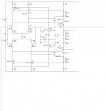
Well....
Attachments
I said: and without using a CMCL, of course
Sorry to realize that you dont like the control loop. But that can bee deletet...
cheers
Ronny
Attachments
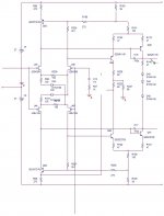
Sorry to realize that you dont like the control loop. But that can bee deletet...
And if you ignore the servo (which is obviously wrong):
http://www.diyaudio.com/forums/soli...s-blowtorch-preamplifier-934.html#post1609863
Two years ago, the same guy analyzed and measured a bootstraped Baxandall pair version, on the now defunct diy-audio-engineering forum (sorry, I don't have the permission to post the schematic). The VAS distortions were also vanishing low (even lower than what Edmond is showing here), but here it's Edmond's output stage that allows going into the ppm range. Without the autobias output stage, the results are not hugely better than a standard Blameless. That's because the standard EF output stage distortions are orders of magnitude larger than the VAS, anyway.
Last edited:
sorry, I don't have the permission to post the schematic
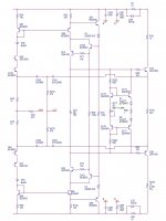
Got it, see attachment.
Attachments
- Status
- This old topic is closed. If you want to reopen this topic, contact a moderator using the "Report Post" button.
- Home
- Amplifiers
- Solid State
- Has anyone seen this front-end before?