With no degeneration the miller local loop is itself "degenerated".
The emitter degeneration will allow for the base/emitter capacitance
to be bootstrapped in respect of the base.
Without this degeneration the said Cbe will be seen as a short to ground
at high frequency , drasticaly reducing the local NFB where it is most needed.
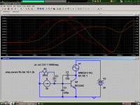
A simple schematic help to understand more easily.
This is not necessarily such a bad thing for common emitter stage, what happens when it gets loaded ??
Wahab, Re does not increase the gain of the stage at HF, rather it blocks it because the Cbe has to discharge through Re before Vbe will change any.
The resistance in this way might be helpful by having a snubber like effect, but the same effect could be had with less consequences by using a base stopper.
The resistance in this way might be helpful by having a snubber like effect, but the same effect could be had with less consequences by using a base stopper.
Actually, Wahab, I think I see what you mean.
Cbc and Cbe act like a positive divider, not unlike a resistive divider, just with capacitors. Some mike preamps do this IIRC.
If there were no Cbe, then modulating Vce would cause an IC modulation that increases with frequency. But because of Cbe, if it is large enough, the capacitive curves will cancel and Ic will be in phase with Vce. But for this behavior Cbe and source impedance usually needs to be large. Something like the BD139 would have this effect I think.
I don't know what this means in relation to your post, but I think my previous comment still stands.
I know that some of Boraomega's designs have a 4.7nF capacitor across the BE junction of the VAS. It is an interesting design decision.
I've been told the BD139 has wildly changing Cj parameters depending on the manufacturer so I'll hazard at say, MJE243. Modern transistors have less Cbe, this may matter.
I've been told the BD139 has wildly changing Cj parameters depending on the manufacturer so I'll hazard at say, MJE243. Modern transistors have less Cbe, this may matter.
Here is an example. I use the BC550C model because it has very low internal capacitance, allowing me to add my own.
With the added Cbe and Cbc values forming a divider, you can clearly see the resistive collector impedance at RF, is different than that at low frequencies. If I take Cbe away, this does not happen. Red trace is with infinite input impedance and orange trace is with 1.2k input impedance, like some amps.
With the added Cbe and Cbc values forming a divider, you can clearly see the resistive collector impedance at RF, is different than that at low frequencies. If I take Cbe away, this does not happen. Red trace is with infinite input impedance and orange trace is with 1.2k input impedance, like some amps.
Attachments
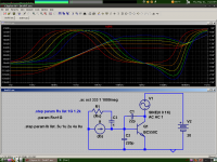
If we make Cshunt, or Cbe, very large, say 4.7n, the RF level gets lower, closer to the DC level. Judging by the anomaly at 10MHz it seems there is an optimal value here.
Red trace is collector response with 220pF Cshunt. Orange is with 4.7nF Cshunt.
Red trace is collector response with 220pF Cshunt. Orange is with 4.7nF Cshunt.
Attachments
Now I would guess, that in this cause, because both Cbe and Cbc respond proportionally to Vce, that in the capacitive divider configuration their nonlinearities will cancel. But this relationship is broken when you give the transistor a low-impedance input. Thus maybe making a case for a non-buffered or even current-drive VAS. Maybe I'm just crazy.
Now I would guess, that in this cause, because both Cbe and Cbc respond proportionally to Vce, that in the capacitive divider configuration their nonlinearities will cancel. But this relationship is broken when you give the transistor a low-impedance input. Thus maybe making a case for a non-buffered or even current-drive VAS. Maybe I'm just crazy.
Hi, must say i was waiting for it ! looking at each stage as a current amplification. The only stage that do not have current amplification is.............. folded cascode.
")
Actually, Wahab, I think I see what you mean.
Cbc and Cbe act like a positive divider, not unlike a resistive divider, just with capacitors. Some mike preamps do this IIRC.
If there were no Cbe, then modulating Vce would cause an IC modulation that increases with frequency. But because of Cbe, if it is large enough, the capacitive curves will cancel and Ic will be in phase with Vce. But for this behavior Cbe and source impedance usually needs to be large. Something like the BD139 would have this effect I think.
I don't know what this means in relation to your post, but I think my previous comment still stands.
It seems to me that given a source with significant output Z , wich is the
case of an IPS , moreover at VHF , phase shift of the VAS output will
increase proportionnaly to frequency with degeneration limited to Re,
while gain will continue to fall further in the -dB since Cbe impeadance
will inevitably decrease with frequency.
With adequate degeneration the VAS output phase shift will
start to stabilise at a given frequency , close to the component Ft ,
never exceding 360° phase shift in respect of the input , that is ,
the device output phase is not over 180° late , implying unconditional
stability of the local loop if ever the global NFB is gone due to clipping
and that the VAS is in some way abandonned to its own behaviour ,
isolated from the rest of the amp.
In real world application this is dependant of the ability to eliminate
any substancial inductance in the layout around the VAS.
Going through sims just show that at VHF the real schematic
is very far from what it ressemble at LF....
Anyway it would be good to have some explanations from
people by there that did dig deeper on this subject.
For one thing, the source impedance to the VAS is never large as long as there is a feedback loop. The source impedance will generally appear resistive, then inductive, then resistive again at the point where the feedback loop loses BW, and then capacitive, as frequency increases.
What you describe with board inductances is essentially a resonance occuring with local inductance. Degeneration will lower the Q of the resonance in this case, and it can be critically damped. So like I said, it acts like a snubber. However I think a base stopper is a better option if you can get away with it. Furthermore, a small 10nF cap to close the VAS output current loop, may do wonders if board inductance is a problem.
I can see that maybe degeneration could be the only way to solve local VAS oscillation in a specific circuit, but this seems like it would be an exceptional and rare event, which shouldn't be thrown in the bin with the majority of cases.
I have very little real-life experience here, so my thoughts should be seen as my best guess.
Last edited:
At the frequencies , as much as 100 to 200mhz , at wich oscillations can occur
NFB is already long gone so to understand what is going on the VAS has to be seen
as an insulated gain stage that oscillate localy.
What then remain are the component intrinsical capacitances and resistances
that will define its dynamical behaviour , possibly an oscillator if there s enough
phase shift and gain from input to output.
As said , without degeneration the device intrinsical gain will stay above unity
while phase already reached 180 excess shift inducing oscillations within the device
itself.
Also the condition for NFB to disapear in an amp can be not only clipping
but simply input signal excessive slew rate.
Can someone check this?
Want to understand this better.
On Edmond's website there is link to the Dymond and Mellor paper on two pole compensation. Two Pole
I think that equation 28 for Rm would have a Q of the two poles as
(Sqrt(BetaRcR1C1C2))/(R1C1 + R1C2 + RcC2)
If we assume Rc >> R1 (say Rc= 40k and R1 = 400)
then Q is approximately
Sqrt(BetaR1C1/RcC2)
The R1C1/RcC2 is about 1/5 so say Sqrt = 1/2
So the Q is of the order of 1/2 Sqrt(Beta)
If the VAS is a pair (as shown in Fig.5) then the effective Beta is approximately half the product of the 2 individual betas. Say transistor beta=140
So the the calculated Q is of the order of 50.
Obviously this is a simplified model that considers only the Fig. 10 circuit.
but it seems inconsistent with the results shown.
It is more in line with Bob Cordell's results.
Have I made a maths slip or is this an accurate analysis of the model?
Best wishes
David
Its interesting to see the matter of TPC and TMC come up...
While Waly's reminder about the stability limitations shared by TMC and TPC is correct, it is important to bear in mind that TPC and TMC are not the same. Some are perhaps misled by their topological similarity of appearance to think they are equivalent..
Cheers,
Bob
Want to understand this better.
On Edmond's website there is link to the Dymond and Mellor paper on two pole compensation. Two Pole
I think that equation 28 for Rm would have a Q of the two poles as
(Sqrt(BetaRcR1C1C2))/(R1C1 + R1C2 + RcC2)
If we assume Rc >> R1 (say Rc= 40k and R1 = 400)
then Q is approximately
Sqrt(BetaR1C1/RcC2)
The R1C1/RcC2 is about 1/5 so say Sqrt = 1/2
So the Q is of the order of 1/2 Sqrt(Beta)
If the VAS is a pair (as shown in Fig.5) then the effective Beta is approximately half the product of the 2 individual betas. Say transistor beta=140
So the the calculated Q is of the order of 50.
Obviously this is a simplified model that considers only the Fig. 10 circuit.
but it seems inconsistent with the results shown.
It is more in line with Bob Cordell's results.
Have I made a maths slip or is this an accurate analysis of the model?
Best wishes
David
that paper is weak - makes a "begging the question" assumption in the model, later skips a couple of steps jumping to the cascode terminaion and thereby misses the opportunity to illustrate a fundamental about amps specifically the cmrr, psrr, Aol relation
“A General Relationship Between Amplifier Parameters, And Its Application to PSRR Improvement” E Sackinger, J Groette, W Guggenbuhl, IEEE Trans CAS vol 38, #10 10/83 pp 1171-1181
a little related discussion around my post: http://www.diyaudio.com/forums/soli...lls-power-amplifier-book-217.html#post2695213
running up a full symbolic hybrid-pi model with the two feedback options shouldn't be hard with modern symbolic math SW - I'd use the Maple engine in a old MathCad (v11) - or I keep saying I want to learn a public domain symbolic tool for sharing work - Sage Math has Macsyma and a pretty printing LaTeX sketchbook
that paper is weak - makes a "begging the question" assumption in the model, later skips a couple of steps jumping to the cascode terminaion and thereby misses the opportunity to illustrate a fundamental about amps specifically the cmrr, psrr, Aol relation
“A General Relationship Between Amplifier Parameters, And Its Application to PSRR Improvement” E Sackinger, J Groette, W Guggenbuhl, IEEE Trans CAS vol 38, #10 10/83 pp 1171-1181
a little related discussion around my post: http://www.diyaudio.com/forums/soli...lls-power-amplifier-book-217.html#post2695213
running up a full symbolic hybrid-pi model with the two feedback options shouldn't be hard with modern symbolic math SW - I'd use the Maple engine in a old MathCad (v11) - or I keep saying I want to learn a public domain symbolic tool for sharing work - Sage Math has Macsyma and a pretty printing LaTeX sketchbook
You are, as usual, a positive mine of information.
In the Dymond and Mellor paper it's the plot of loop gain in Figure 11. that really surprises me.
It seems inconsistent with their own equation and also Bob Cordell's book.
At least the model is more or less consistent with Bob Cordell, even if it is a bit weak.
Thank you very much for the reference to the relationship paper.
I will read it and think a bit before any reply.
Best wishes
David
“A General Relationship Between Amplifier Parameters, And Its Application to PSRR Improvement” E Sackinger, J Groette, W Guggenbuhl, IEEE Trans CAS vol 38, #10 10/83 pp 1171-1181
Had a quick look at the paper. Seems to use a heavy hammer to crack a peanut.
You hardly need to quote gauge invariance to make the point that potential is arbitrary.
Doesn't seem very relevant since it deals only with amps suspended between 2 rails, typically op-amps.
Practically any audio power amp will have an earth reference, so you lose "gauge invariance" as they would say, and the central thesis of the article is inapplicable. Have I missed some point?
On the plus side- After 25 years, it's the first time I have ever used my Gauge Theory text (K. Moriyasu) except as a bookend. I had almost lost hope! And Dirac <bra|ket>s, whooh! <
|>Best wishes
David
clearly the Physicists were having with/making of fun of the EEs
while power amps have gnd available it often isn't used in the compensation so the relations apply to many "Lin" decendants
and the paper spells out your options - moar gain, change topology to ref compensation to gnd, or full differential (which often has to have explicit common mode control loop) - without the insights there is lots of flailing around in the dark
gauge invariance still probably won't be a hot cocktail party topic most places
Hello Dave,
Thanks for your PM. My apologies for not replying sooner; I have been on holiday. I'm glad you enjoyed reading the paper; I hope you don't mind me replying to you in this thread; there are plenty of folks in the thread considerably cleverer and more experienced than me who may be able to shed light on this conundrum.
I will admit that the paper certainly has some weaknesses; the model used to derive the transfer equation is as simple as it could possibly be. Fortunately, the main insights delivered - the ULGF frequency, zero frequency, current requirements of the VAS/TIS and input stage, that the large and small caps should have their positions reversed relative to the suggestions of Self and Slone, and the fact that the value of R1 only has an effect on the loading of the input stage and a higher value makes the loading worse - are all valid regardless of the simplicity of this model.
Actually, by far the biggest weaknesses of the paper are some things jcx didn't mention (perhaps deliberately in order not to be overly harsh):
Now, on to your actual question!
Yes, I agree with your analysis of my analysis: a much bigger Q is predicted by the equation than what is seen in the simulator. Referring to figure 5 from the paper, the transistor model numbers are:
If you want, I can provide the spice models used (they're nothing special).
Also, upon double-checking it appears that the simulation used to deliver the curves in figure 11 was run with the amplifier output loaded with 8R. If the load is removed the Q of the poles does increase, but is still nowhere near 50.
So, according to a SPICE simulation, the Q of the poles is very much lower than that predicted by the simple model. Presumably this is because, as discussed earlier in the thread, at frequencies before the feedback around the VAS/TIS has really "kicked in", the stage is behaving more like a VAS (i.e., volts in, volts out), whilst the model assumes TIS operation from DC.
Certainly the Q of the poles is something that puts some people off TPC. As noted in my paper, you can introduce a further pole zero pair by adding a capacitor in series with the TPC resistor. If the loop gain poles have a high Q, by selecting the appropriate additional capacitor value, you can make the loop gain look like it just has two critically damped poles (plus the zero at higher frequency) rather than three poles and two zeros.
Finally, it bears emphasising that the frequency and Q of the loop gain poles are very sensitive to VAS/TIS transistor beta (and also sensitive to output stage beta) and will therefore vary dramatically from one instance of an amplifier to another. One should ensure stability at the extreme of Q (maximum VAS/TIS and output stage betas, no load on amp output), and then make sure everything is still happy at the other extreme (minimum transistor betas and heaviest amplifier loading).
Well, that's my take on it and I look forward to further discussion!
Thanks for your PM. My apologies for not replying sooner; I have been on holiday. I'm glad you enjoyed reading the paper; I hope you don't mind me replying to you in this thread; there are plenty of folks in the thread considerably cleverer and more experienced than me who may be able to shed light on this conundrum.
I will admit that the paper certainly has some weaknesses; the model used to derive the transfer equation is as simple as it could possibly be. Fortunately, the main insights delivered - the ULGF frequency, zero frequency, current requirements of the VAS/TIS and input stage, that the large and small caps should have their positions reversed relative to the suggestions of Self and Slone, and the fact that the value of R1 only has an effect on the loading of the input stage and a higher value makes the loading worse - are all valid regardless of the simplicity of this model.
Actually, by far the biggest weaknesses of the paper are some things jcx didn't mention (perhaps deliberately in order not to be overly harsh):
- The proposed method of simulating loop gain doesn't work above the ULGF or at very low frequencies (<5 Hz) (note this means it cannot be used to predict gain margin). However, for 5 < f < ULGF, the method does work better (gives more accurate results) than the "break loop and insert great big inductor" method and can be used to observe the "correct" behaviour of the poles, the zero, the ULGF and the phase margin. This has been verified by comparing the method to the only proper way to simulate loop gain: with the General Feedback Theorem, or a close second, with Tian's method. Sadly I had never heard of Middlebrook or Tian at the time I wrote the paper.
- It is not discussed that it is important to ensure that the inner feedback loop (in addition to the global feedback loop) is stable; it is possible that when cascodes are added to the input stage and VAS/TIS that the inner loop becomes unstable.
Now, on to your actual question!
Yes, I agree with your analysis of my analysis: a much bigger Q is predicted by the equation than what is seen in the simulator. Referring to figure 5 from the paper, the transistor model numbers are:
- Q1 = Q2 = BC857A
- Q3 = Q4 = BC860A
- Q5 = Q6 = BC847B
- Q7 = Q8 = BC850B
- Q9 = Q11 = KSC2690A
- Q10 = 2N5401
- Q12 =KSA1220A
- Q13 = MJL3281A
- Q14 = MJL1302A
- R15 = 50R
If you want, I can provide the spice models used (they're nothing special).
Also, upon double-checking it appears that the simulation used to deliver the curves in figure 11 was run with the amplifier output loaded with 8R. If the load is removed the Q of the poles does increase, but is still nowhere near 50.
So, according to a SPICE simulation, the Q of the poles is very much lower than that predicted by the simple model. Presumably this is because, as discussed earlier in the thread, at frequencies before the feedback around the VAS/TIS has really "kicked in", the stage is behaving more like a VAS (i.e., volts in, volts out), whilst the model assumes TIS operation from DC.
Certainly the Q of the poles is something that puts some people off TPC. As noted in my paper, you can introduce a further pole zero pair by adding a capacitor in series with the TPC resistor. If the loop gain poles have a high Q, by selecting the appropriate additional capacitor value, you can make the loop gain look like it just has two critically damped poles (plus the zero at higher frequency) rather than three poles and two zeros.
Finally, it bears emphasising that the frequency and Q of the loop gain poles are very sensitive to VAS/TIS transistor beta (and also sensitive to output stage beta) and will therefore vary dramatically from one instance of an amplifier to another. One should ensure stability at the extreme of Q (maximum VAS/TIS and output stage betas, no load on amp output), and then make sure everything is still happy at the other extreme (minimum transistor betas and heaviest amplifier loading).
Well, that's my take on it and I look forward to further discussion!
Certainly the Q of the poles is something that puts some people off TPC. As noted in my paper, you can introduce a further pole zero pair by adding a capacitor in series with the TPC resistor. If the loop gain poles have a high Q, by selecting the appropriate additional capacitor value, you can make the loop gain look like it just has two critically damped poles (plus the zero at higher frequency) rather than three poles and two zeros.
Thank you for your helpful and informative reply. I need to think a lot before I can make a considered response.
One question does come to mind immediately. You put a capacitor in series with the TPC resistor. Bob Cordell puts a capacitor in parallel across the TPC capacitors. Are these two methods equivalent? I should be able to solve this but some of the TPC results are not obvious, as you have very valuably pointed out, so I would appreciate your comment.
Best wishes
David
- Status
- This old topic is closed. If you want to reopen this topic, contact a moderator using the "Report Post" button.
- Home
- Amplifiers
- Solid State
- Has anyone seen this front-end before?