http://www.sealelectronics.com/kits/images/OPTI1001.pdf
Checking my limited knowledge: to decrease gain you need to increase R17 to say 470R (and maybe increase R2 to 22k)?
There are 10pf caps on the mosfet gates in the latest OPTI-MOS rev. (oct 2003), c16 has a series 270R added, input diff pair changed to MPSA56, input protection D1&D2 are gone, and some more layout/resistor changes. I only have the schematic on paper, can't post it here...
Did stripping the protection circuit out had any benefic effects? I guess I can find out by myself by just removing q17 & q 18.
I'm also very curious about the mosfet source followers... if you keep the prot circuit in, decreasing source res values to .22 will get you more current capability before the prot kicks in? What if I increase R25 & R32 to 100R? Any other considerations here? The mosfets are not that well matched (Randy said it doesn't matter if the mosfets are matched or not) so I don't know if this would be a good idea...
Gain is simply (R20 + R17) / R17
R2 and R20 determine the input resistance and need to be the same value.
I can't say if there's any sonic benefit to removing the protection circuit becuase I took it all out during my process of elimination and have not put it back.
Do you mind describing the other layout and changes you've hinted at, I would really like to know!
Nick
Re: revised schematics
Randy is fully aware that professional designers can read his books, copy his circuits, and get into business. I get the feeling that he's not too possessive about that.
Of course, I don't have any authority to speak on his behalf... these are all my opinions.
I am not sure that there will be any ethical or legal problem if you discuss the mods here. Randy has published the basic schematic with full explanations in a book and on his Website. And he's freely answered questions posted by any of his readers or builders. I am quite sure he wants to see his insights and experience benefitting us amateur builders. If we were aiming to compete with Zus Audio professionally, it would be a different matter. Even in that case, I feel he's basically a teacher, and he's not interested in being ultra-careful with tips and tweaks to his published circuits. Whatever he does for Zus Audio is not published, and I wouldn't discuss those circuits here even if I had access to them.MichaelB said:I've contacted Mr. Slone two weeks ago to get some answers on parts used in the OptiMOS design. His extreme friendly answer had revised schematics for the commercial versions (the ZUS-Amplifier) of the OptiMOS, both 200W/400W and a new 800W Version attached.
For obvious reasons I can't post them in this forum.
Randy is fully aware that professional designers can read his books, copy his circuits, and get into business. I get the feeling that he's not too possessive about that.
Of course, I don't have any authority to speak on his behalf... these are all my opinions.
Yes, please do. I think there's enough interest among us to do a revised OptiMOS, and we're all amateur builders... Randy would probably not mind us discussing it.lucpes said:I'll ask Randy Slone for permission to post the updated schematics here...
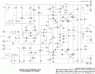
Revision 4 OPTI-MOS units
Designer: G. Randy Slone, SEAL Electronics, http://www.sealelectronics.com
These amplifiers are the 'heart' of the upcoming commercial ZUS
amplifier series, more info coming at http://www.zusaudio.com
Designer: G. Randy Slone, SEAL Electronics, http://www.sealelectronics.com
These amplifiers are the 'heart' of the upcoming commercial ZUS
amplifier series, more info coming at http://www.zusaudio.com
Attachments
Here's the image for quick view, see the bigger sized one in the post above.
Revision 4 OPTI-MOS units
Designer: G. Randy Slone, SEAL Electronics, http://www.sealelectronics.com
Revision 4 OPTI-MOS units
Designer: G. Randy Slone, SEAL Electronics, http://www.sealelectronics.com
Attachments
millwood said:did anyone see the tantalum caps on the input?
")
I must confess that it sounds lots better without those.
Attachments
In another context, I ran some SPICE models where the oppossed zeners (see the ealier Opti-MOS schematics) at the input plus 10uF of input capacitance dominated the noise floor and swamped distortion until you reached fairly high frequencies. Objectively, it didn't mater much since the figure were so low anyway but it just felt irritating that after a certain amount of effort to layout very low noise and distortion design that these two unglamorous items would be the limiting factor. I figured out that increasing the capacitance (or taking the brave step of removing it) and removing the zeners made a big percentage inprovement in THD+N. But to reiterate 50% of very, very little is still very, very little. If you get my drift.
On the new schematic it looks like Slone moved the function of the zeners (over-voltage protection for the input transistors) to the switch diode pair between the bases of the same transistors. I'm not convinced yet that the low noise transistors selected gain you more than you loose by having to add protection components.
It also appears that protection transistors have been added to the VAS. I somehow thought that was only needed with an enhanced beta design. Maybe not . . .
Overall, as Slone tries to get this closer to commercial production it looks like he's trying to mitgate even minor and improbable problem areas.
sam9 said:
On the new schematic it looks like Slone moved the function of the zeners (over-voltage protection for the input transistors) to the switch diode pair between the bases of the same transistors. I'm not convinced yet that the low noise transistors selected gain you more than you loose by having to add protection components.
Obviously the diodes are suppose not to conduct until you overload
the input, so the question is, does a diode generate noise even
when not conducting? Hm, I suppose it does if you measured
such an effect for the earlier zeners?
sam9 said:(...)It also appears that protection transistors have been added to the VAS. I somehow thought that was only needed with an enhanced beta design. Maybe not . . . (...)
It looks like when there's a short at the output, and if the current limiting transistor Q13 weren't there, the max current in Q19 (and Q14 and Q15 as well) wouldn't be reached until Q19 saturated. Since the base of Q15 is at half the supply voltage in this case, its collector can't go much above that. So the max current in Q19 would be about (32.5 - 0.7 - 0.3) / 150 = 210 mA. This assumes Vce(sat) of Q19 is 0.3 and the voltage across D6 is 0.7. This would probably burn up Q14, as it would be dissipating about 6.3 Watts (since it would have about 30V across it). So Q13 saves the day in this case by limiting the current to about 26 mA.
Christer said:
Obviously the diodes are suppose not to conduct until you overload
the input, so the question is, does a diode generate noise even
when not conducting? Hm, I suppose it does if you measured
such an effect for the earlier zeners?
Zener diodes always conduct some small amount of current, even at voltages below their rated breakdown. They are not ideal components, but are handy within their limitations. Even at their rated voltage, they have a dynamic resistance which means the zener voltage changes with appied voltage.
So as voltage clamps across the input, you must accept their limitations to get their benefits. In the musical instrument amp world, where line voltages can be put on inputs, they save the amp from total destruction at a cost of a negligible increase in distortion. For home use, they are not appropriate and may be dispensed with. Slone makes their purpose clear in his book, they typically are only for musical instrument input protection circuits, used together with extensive frequency filtering also.
I believe the back to back signal diodes across the bases of the input pair have been used to protect op amp inputs for years. Diodes are not perfect devices, and will themselves cause distortion while preventing damage to the input pair. This is the right tradeoff for a musamp, not so good for home hifi, in my opinion.
While testing amps, I have damaged the input pairs by overdriving the inputs above 6VAC. They get leaky and have higher offset voltage, a not uncomman defect in amps I repair, so I think this happens in use quite a bit. This validates that there is a practical benefit to adding some protection against that kind of abuse -- it does happen, so plan to survive if you expect overvoltage inputs to occur in normal use.
I'm not sure I understood this correctly, so please can you help me? I was wondering what if I connect eight signal diodes in two series-chains of four each, between input and signal-ground. Each chain of 1N4148 will have four diodes, hence will conduct only when the potential difference will go beyond about 2.4V. Will such diodes also introduce distortion?slowhands said:I believe the back to back signal diodes across the bases of the input pair have been used to protect op amp inputs for years. Diodes are not perfect devices, and will themselves cause distortion while preventing damage to the input pair. This is the right tradeoff for a musamp, not so good for home hifi, in my opinion.
And what about the 1N4007 diodes that are used between the speaker output and the supply rails of the power amp? Will those also cause distortion?
I'm really new to all this, so some of my questions may sound stupid. Sorry.
Originally posted by Nick Walker
Can anyone explain why R6 is 2k7 whereas R18 is 1k, I don't understand why they are not the same.
It has to do with the VAS (Q14) loading the input stage. By having R18<R6, the designer is trying to maintain equal current in the two legs of the differential.
Hi,
I'm planning on building a Slone (fig 11.4) amp too. I just see some problems, which are porbably allready solved by you guys.
The text states at page 338 that I can replace the Q12 and Q14 (MJ series) with 2S series, but the schematic allready lists 2S sersies, why?
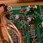
Is there a reason for the fact that fig c.6-8 doesn't match with the photo on page 336?
R33 is connected to R34 etc with a wire. Judging from the PCB artwork fig c.7 this is a normal sized wire, isn't that suboptimal?
I hope someone can answer these questions. If this board is OK, then I'll probably order it from SEAL. I don't have the experience to design my own at the moment.....
Thanks in advance,
Remco Poelstra
I'm planning on building a Slone (fig 11.4) amp too. I just see some problems, which are porbably allready solved by you guys.
The text states at page 338 that I can replace the Q12 and Q14 (MJ series) with 2S series, but the schematic allready lists 2S sersies, why?
Is there a reason for the fact that fig c.6-8 doesn't match with the photo on page 336?
R33 is connected to R34 etc with a wire. Judging from the PCB artwork fig c.7 this is a normal sized wire, isn't that suboptimal?
I hope someone can answer these questions. If this board is OK, then I'll probably order it from SEAL. I don't have the experience to design my own at the moment.....
Thanks in advance,
Remco Poelstra
Thoru,
I called Slone in the early part of last year to buy 11.4 boards. He said that due to the time he was spending with ZUS-Audio, the only boards still avaialable were the Opti-MOS. I went ahead and laid out my own double sided boards. It took three trys to get it right but the results are a very nice amp. If you are able to start over a couple of times without getting discouraged it is a good learning experience.
Some of the learning involved just getting better with the layout software. The rest mosatly involved learning to keep the input and VAS sections far, far away from the output. The 11.4 is a CFB and is subject to mysterious oscillations (benign and otherwise). In addition to board layout two things were a real help to getting it going. 1-well shildieded input lines; I cut up some interconnect cable that has a sturdy woven copper shield and 2- move the output inductor (+5W resistor) and the zobel circuit off the PCB and closed to speaker terminals. If you do this watch the location of the output inductors as they can inject cross talk into the other channel as well as add feedback back into your input. Keeping them at a couple of inches away from anything is a good idea.
Hi,
Thanks for your reply.
Apart from the fact that I like to concentrate my learning on other things (it's my first amp and high power circuit in general that I build), I like mostly to keep the costs low. I actually don't have money to build an amp, so I prefer not to have to start over and over again. But if it's the only solution to go than I'll do it that way. I've to learn it one day or another.
Thanks for the tips so far, I hope it saves me one or two tries.
Remco Poelstra
Thanks for your reply.
Apart from the fact that I like to concentrate my learning on other things (it's my first amp and high power circuit in general that I build), I like mostly to keep the costs low. I actually don't have money to build an amp, so I prefer not to have to start over and over again. But if it's the only solution to go than I'll do it that way. I've to learn it one day or another.
Thanks for the tips so far, I hope it saves me one or two tries
.Remco Poelstra
mcp said:
It has to do with the VAS (Q14) loading the input stage. By having R18<R6, the designer is trying to maintain equal current in the two legs of the differential.
Thanks mcp. I did some simulations on Spice and that works, but the change is small about 6uA difference change or 2.1%, going from 1k to 2.7k, however the greater difference seems to be the ability to supply more base current to the VAS stage which is up 60uA or 337%
Hello Nick
Yes, your Spice modelling is correct - an improvement in base current to the VAS.
What is happening in circuits of this nature is that the VAS is "zapping" the diff leg. By making the legs asymmetrical, more current is able to flow through the R1K leg, thus compensating for the "loading" on the 2K7 side.
This technique tries to emulate current mirrors.
- Status
- This old topic is closed. If you want to reopen this topic, contact a moderator using the "Report Post" button.
- Home
- Amplifiers
- Solid State
- Has anyone here built a Slone Amp or a Tigersaurus?