Peter Daniel said:I would be much more concerned with via than a T. There is no problem running this trace directly between pads, without the need for a T. I wouldn't recommend mixing 2 layers for that.
This is a NFB system. The output should be taken from the same point that the FB is sampled from. That point is R1. The current flowing in the T shaped track will cause voltage variations, which equals distortion. The currents will be measured in amps, and the distortion will be easily measured, and perhaps audible. This in itself might not be a big deal, but when it's easy to fix, why not?
The via will not cause problems because it means the output will be taken from R1. Sure, it might add some resistance, but this will be swamped by just the tolerance of R8.
Peter Daniel said:As to the output ground 200mill won't make a difference in performance, but it will make big difference in how easy it is to run the connection wire. I don't care for perfect symetry. I care much more for convenience.")
Sorry - I don't see how moving OG will alter this. I proposed moving it to between SQ and OUT - that it, move it south, then east a bit so that it's directly above the OP pad. This will make wiring simpler because you can group (or twist) the OP wires. It means altering the blue output trace slightly, but that's all. Again, it's easy to do, and will have a positive effect on the performance. Why not?
Peter Daniel said:The spacing it's done here on purpose. Those are not Krell boards where everything is lined up and spaced perfectly. The board accomodates Caddocks, but I have strong feeling that Rikens will be better here, so this extra space allows to mount Rikens as well (in vertcal position). You wouldn't mind putting them this way? After all those extras on the leads are part of 3-D layout, (popularasied by Jonathan Carr)
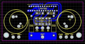
Sorry - you can't convince me that the uneven spacing was deliberate. This is just how things look after the first "pass" at placing components without using a horizontal grid. If it was deliberate, why is R4 so very close to R8, causing the blue SG trace to almost touch the output node. BTW, this is bad, because the current in the output node could easily induce currents in the SQ, causing yet more distortion (although this partly depends what the IC does with it's GND pins, and I can't comment because I've yet to see an internal schematic).
I wouldn't like to mount resistors vertically - this is universally bad practice on a PCB. What JCarr is quite different - he uses this technique to shorten signal path lengths. I was planning to use 1/8 watt resistors that mount horizontally, bit would consider using those square-body resistors that I've seen (sorry - I'm not up with the brand names)
Peter Daniel said:Even if you place those resistors closer to the chip, you still have to run the connection wires around the board (this makes those wires longer) so I don't see much difference here. And anyway, there is no space to place those resistors there. Again having conveniently placed input access points on the board was major deciding point.
If you moved the resistors nearer the IC, the traces between resistor and IC gets shorter. The trace from I/P pad (which doesn't move) becomes one of the two traces that you currently have. You might have mis-understood the point - in terms of suscecpability to RF pickup, the traces between IC and resistors are more sensative because they are at a higher impedance, so these should be "protected" or shortened. The trace from IP pad is at a lower impedance, so is less of a problem. Lookup guard-traces in any precision op-amp datasheet.
Peter Daniel said:Regarding the "trace from R6 looks very close to the R9", look how close those are on IC pins
You're missing the point - sure the pins are close together on the IC, but look at how National allocated them - the OP pins are seperated from the IP pins by power lines. Indeed, this is normal practice in most amplifier ICs. Again, how much effort would it take to move that trace south a bit? If there's even the slightest doubt about something, and it's easy to fix, then why not?
Peter Daniel said:It took at least 5 days and countless hand drawings to finalize that layout.
I'm still working on a DAC (for almost a month) before committing to final layout.
So be asured that a lot of thought went into those amp boards. Also, we ride on experience gained with a previous version, which tested by hundreds brought only positive feedback
I'm not suggesting that you've not spent a lot of time on this. However, I took quite a lot of time to reply to you, and suggested some genuinely simple things that you missed. I could have suggested lots of other things, but realised that you don't want to re-design the whole PCB at this stage. I thought I was being helpful - the suggestions were based on my experience and understanding of the theory - which is just as valid as your original input, even though you don't seem to think so.
Sorry if that's harsh, but despite the use of smileys, the tone of your replies is dissmisive. In the time it took you to start replying, I can't believe that you even had time to read the message properly, let alone think carefully about a response - you must read very quickly
As I keep saying, if there's even the slightest doubt about something, and it's easy to fix, then why not? It's this attention to detail that makes a product unique and rewarding.
YMMV
Best regards,
Mark
PS What does BrianGT think?
mhennessy said:PS What does BrianGT think?
Mark,
Thanks for the your comments on the layout. I spoke with Peter, and I will make some revisions to the design and post a new screen shot this evening. I find your concerns to be valid, and I will see what I can do.
--
Brian
Via is not an option in a well designed, audio board, sorry.
Besides replying on a fast, I aslo took your suggestions seriously, and will try to implement, togethe rwith Brian, to the best degree. But some things are either negligable, or simply not possible.
You mught not like vertical standing resistors from aestchetical point, but if they sound better, I will not loose sleep over that. Those resistors are vertical in order to maximise the width of ground plane. You can always use smaller size regular ones , or Caddocks.
Re: 4 ohm speakers ok for bridged mode?
The amplifier board uses 2 channels in parallel with the LM4780, so each channel would see 8 ohms on the amplifier pcb if you are just using one pcb. When you bridge two amplifier boards, each amplifier board will see half of the load, but since there are 2 channels in parallel on each board, each channel (4 of them used in a bridged setup), will see a 4 ohm load.
--
Brian
garbage said:any ideas if it would be ok to use a 4ohm speaker for bridged mode?
i understand that each amp(when bridged) will see the speaker as a 2ohm load per channel, but want to know if the lm4780 can take such a load.
The amplifier board uses 2 channels in parallel with the LM4780, so each channel would see 8 ohms on the amplifier pcb if you are just using one pcb. When you bridge two amplifier boards, each amplifier board will see half of the load, but since there are 2 channels in parallel on each board, each channel (4 of them used in a bridged setup), will see a 4 ohm load.
--
Brian
mhennessy said:
I'm not suggesting that you've not spent a lot of time on this. However, I took quite a lot of time to reply to you, and suggested some genuinely simple things that you missed.
I didn't miss anything, Brian did the final layout, following my earlier suggestions. If I modified it, it might have look differently, as well. My points are valid, regarding major design decisions, not small details.
mhennessy said:
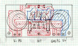
Sorry - you can't convince me that the uneven spacing was deliberate. This is just how things look after the first "pass" at placing components without using a horizontal grid. If it was deliberate, why is R4 so very close to R8, causing the blue SG trace to almost touch the output node.
The spacing between those resistor should be according to that scetch. Only than installing Rikens present's no problem. This spacing is deliberate. It seems like Brian didn't do it quite accurately though.
Attachments
BrianGT said:Mark,
Thanks for the your comments on the layout. I spoke with Peter, and I will make some revisions to the design and post a new screen shot this evening. I find your concerns to be valid, and I will see what I can do.
--
Brian
Thanks for offering to consider my suggestions, Brian. That's all I ask
Peter Daniel said:Via is not an option in a well designed, audio board, sorry.
Genuine question - Can I ask why?
Peter Daniel said:Besides replying on a fast, I aslo took your suggestions seriously, and will try to implement, togethe rwith Brian, to the best degree. But some things are either negligable, or simply not possible.
I only wanted you to consider them as possible options. Can you at least understand why the speed and tone of the reply didn't suggest this?
Peter Daniel said:You mught not like vertical standing resistors from aestchetical point, but if they sound better, I will not loose sleep over that. Those resistors are vertical in order to maximise the width of ground plane. You can always use smaller size regular ones , or Caddocks.
My concerns for this are not aesthetic - I was thinking about the (real) possibility for RF pickup again. I've worked in different dissiplines over the years, and I guess that certain experience makes you worry about certain things...
So, have you found that mounting resistors vertically improves the SQ? Or, are you thinking of comparing different sorts? For example, I quite like 0.1% RN55's, which would have to be mounted vertically on this PCB - if I compared these to standard quality miniature 1/8W resistors (mounted horizontally), would the audible differences be due to the component or mounting method?
Best regards,
Mark
Peter Daniel said:
The spacing between those resistor should be according to that scetch. Only than installing Rikens present's no problem. This spacing is deliberate. It seems like Brian didn't do it quite accurately though.
OK - I take your point, although it looks to me like that spacing was to accomodate the blue ground traces - something that isn't an issue with the latest layout.
Also, can I compliment you on your perfect output noding
I'm looking forward to seeing (and eventually hearing) the finished product. Thanks to you and BrianGT for all your work!
Cheers,
Mark
As of now, I'm already working on improving layout based on your suggestions.
Spacing of those resistors is not really desirable (as blue ground trace would be easier to run) but I need that space.
I never seen vias on well implemented audio boards, you can see them in digital a lot though. Aleph X group purchase board was designed with vias, but it was questioned initially, and whwnever I look at that, I think to myself that it could be done differently. To me, via connection is a waek point in a signal path and I never even consider it from pure audiophile POV. Using it is conveneient though.
Regarding vertical resistors, this is not really standard option for that board, Caddocks can be easily used here, but I think that Rikens will sound better (they do on 3875 board) and I wanted to allow placing them here, even at the cost of vertical arrangement. I personally also don't like that way to mount resistor, but inn some cases it is a calculated compromise. In this particualr layout, using Caddocks, leaves more space for running uninterupted ground plane, so I opted for Caddocks (or Vishays) as it looks good and it's a small package. But in my personal amp, I wil be probably using Rikens here. Doen't treat it as inproperly mounted resistor, treated as a resistor with additional trace attached in 3-D space. To me it doesn't make any difference. Running extra trace in air is worth of widening the ground plane.
Regarding the other two resistors (the series input connection), it would be nice to place them closer to the chip, but then the ground returne path is getting longer, (as you can't move all resistors from lack of space) so I don't know if anything is gained by that.
I reply fast, because I already have al lthe answers ready. I asked those questions myself many time when doing that layout.
However I agree that there is a room for improvement here, and whatever possible, it will be done(this ones for real)
Spacing of those resistors is not really desirable (as blue ground trace would be easier to run) but I need that space.
I never seen vias on well implemented audio boards, you can see them in digital a lot though. Aleph X group purchase board was designed with vias, but it was questioned initially, and whwnever I look at that, I think to myself that it could be done differently. To me, via connection is a waek point in a signal path and I never even consider it from pure audiophile POV. Using it is conveneient though.
Regarding vertical resistors, this is not really standard option for that board, Caddocks can be easily used here, but I think that Rikens will sound better (they do on 3875 board) and I wanted to allow placing them here, even at the cost of vertical arrangement. I personally also don't like that way to mount resistor, but inn some cases it is a calculated compromise. In this particualr layout, using Caddocks, leaves more space for running uninterupted ground plane, so I opted for Caddocks (or Vishays) as it looks good and it's a small package. But in my personal amp, I wil be probably using Rikens here. Doen't treat it as inproperly mounted resistor, treated as a resistor with additional trace attached in 3-D space. To me it doesn't make any difference. Running extra trace in air is worth of widening the ground plane.
Regarding the other two resistors (the series input connection), it would be nice to place them closer to the chip, but then the ground returne path is getting longer, (as you can't move all resistors from lack of space) so I don't know if anything is gained by that.
I reply fast, because I already have al lthe answers ready. I asked those questions myself many time when doing that layout.
However I agree that there is a room for improvement here, and whatever possible, it will be done
(this ones for real)Peter Daniel said:Regarding the other two resistors (the series input connection), it would be nice to place them closer to the chip, but then the ground returne path is getting longer, (as you can't move all resistors from lack of space) so I don't know if anything is gained by that.
Thanks for the reply. It had never occurred to me that vias could be a week point, because they are no worse than a standard thermal relief in a ground plane, but I would agree that it's normally good plactice to keep signals on one side of the board...
Anyway, I'm not sure if I explained the two-resistors thing clearly enough, so I've modified the .gif (I don't have access to PCB CAD here) - the image is messy, but you'll hopefully get the idea. Perhaps putting them there causes physical problems (if they're vertically mounted, for example)? Note that I also took the liberty of following this through to the logical conclusion - I moved R4 to occupy the space left by R6/7, improving the earth trace that I mentioned earlier.
Having said all of that, I prefer the aesthetics of 5 little resistors in a neat row
Attachments
![pcb-layout[1].gif](/community/data/attachments/2/2058-2d6177643b7c276ec15269ae05c7aab5.jpg)
But do you see how input trace extended? So nothing is really gained except for unning shorter 2 traces and longer a single trace. Also the SG node is chanched and I don't think if for better.
I modified resistors spacing a bit and some traces, addressing T connection and trying to simplify input traces (they are shorter now). I still didn't do adjust polygon but connected SG and OG with a single blue trace.
I modified resistors spacing a bit and some traces, addressing T connection and trying to simplify input traces (they are shorter now). I still didn't do adjust polygon but connected SG and OG with a single blue trace.
Attachments
Peter Daniel said:But do you see how input trace extended? So nothing is really gained except for unning shorter 2 traces and longer a single trace.
Yes, but the point you're missing is the traces between the resistors and IC are the vulnerable ones! Sure, the input trace is perhaps slightly longer, but remember that this trace is just an extension of the input wiring from the rear panel (or DRV134 PCB). This trace is at low impedance, and less prone to interferrence.
Peter Daniel said:Also the SG node is chanched and I don't think if for better.
The earthing is actually better with this, but as it's the signal earth and no currents are flowing here, this is a mute point.
Peter Daniel said:I modified resistors spacing a bit and some traces, addressing T connection and trying to simplify input traces (they are shorter now). I still didn't do adjust polygon and forgot to connect SG and OG with a single blue trace.
Yes, this is much better, and addresses most of my concerns.
The biggest problem with my input resistor move is the uncomfortable aesthetic of those two resistors all out on their own (although you did say that you prefered sound to aesthetics
)... While I was playing, I couldn't resist improving the signal earthing further (possible alternative route shown in green, although I prefer the blue)Attachments
![pcb-layout[1].gif](/community/data/attachments/2/2084-ab32370e2a3b59180d7757c56d3475b2.jpg)
Like this, but I'm not sure if it's really better. I'd rather prefer to have input signal and input ground side by side, and moving OG by 200mil won't make any observable difference, IMO.
Another issue is running the connections wire. Going away from the board I would also prefer to have them spaced, and this arrangement doesn't relly allow it (if you know what I mean).
Another issue is running the connections wire. Going away from the board I would also prefer to have them spaced, and this arrangement doesn't relly allow it (if you know what I mean).
Attachments
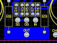
Peter Daniel said:With regards to have OG centrally positioned, I think it could be swaped with SG pad for more central placement.
Yes, I'd agree with this
Although the two wires from the input signal "straddle" the OG, which might be uncomfortable. But, these amps are capable of passing a lot of current, and every mil is important - so it's a compromise I'd seriously consider. But, I'm using these in bridged mode, so as I said before, I don't personally feel that strongly about it.
Hometime now - look forward to seeing the updates tomorrow morning
Best regards,
Mark
mhennessy said:
although I prefer the blue)
If you check pin out on the chip, the pin where you connected blue trace is NC. The best connection point for ground path would be your left, green trace.
Regarding long traces from input resistors to the chip, I might be concerned with them, but obviously it wasn't a concern of National design team when they made evaluation board. Those traces are even longer on their board.
- Status
- This old topic is closed. If you want to reopen this topic, contact a moderator using the "Report Post" button.
- Home
- Group Buys
- Group order of non-inverted LM4780 pc boards? Anyone interested?