Hi JCX,
Geoff's website is a marvellous source for JLH information, but you are modelling an idealistic JLH output stage that is powered by two current sources, and this runs differently to one that is energised by a single current source or a bootstrapped collector resistor.
The original JLH-69 had quite different driver collector and emitter resistors, the later ones a single 'current source' approach, so the output stage would be less well gain balanced between output halves, than either the current source stage you are modelling or mine with equalised resistors. JLH relied upon a high value base-emitter resistor for the lower output transistor.
I have not asserted and do not assert a 1MHz pole, but there is always one value of NFB sensing capacitor for any given type of circuit that is necessary to ensure fast but stable NFB loop control in the presence of loudspeaker generated back EMF. No 'C' at all can cause - brightness, too high a 'C' - dullness, also without the correct value of 'C' a toneburst will lead to the alternating output voltage zero being shifted away from the quiescent zero.
It is not easy to use any kind of fet to advantage in a JLH output stage, because the phase splitting does not remain 180 degree separated with increasingly high frequency - oscillation breaks out. In real life I have run my 25W circuit without the 22pF capacitor and it remains stable, but I feel that you really do need to build your circuit before discussing more hypotheticals, because your 22pF arrangement will make the non-NFB compensated phase change worse. Do you not see an awful amplitude-phase plot when you simulate your #Post38 circuit ? Also when you talk about increasing the NFB level, by how much ?
Cheers ............. Graham.
Perhaps poor output transistor modeling is exaggerating the push-pull current division asymmetry in the output transistors, but Goeff’s site certainly warns that you cannot get the 2X Iq output expected from balanced push-pull class A with real jlh output stages
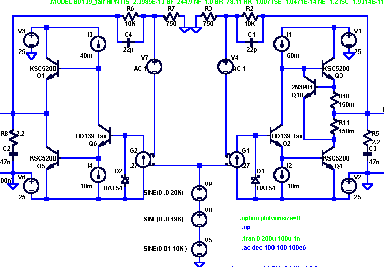
I’ve been fooling around in sim with a class A bias scheme that can enforce symmetric current division that turns out to fit easily to the jlh output
Q10, R10,11 form a classic 2 transistor feedback current source with Q3,
Iq = Vbe(Q10)/(R10+R11)
The upper bias current source is increased to provide working current for Q10 (~ 14 mA in this sim) – this has to be large enough to supply excess output Q Ib to compensate for the hfe mismatch of the output Qs over their operating range
In the sim this local current sensing bias scheme manages to match +/- Ie symmetry to 3% while setting the output Iq without repeated iterative bias adjustments
The current in Q10 is largely 2nd harmonic, but interestingly this results in raised 3rd harmonic output distortion – increased symmetric distortion can be expected to lead to increased odd harmonics
{having problems with photobucket so you have do it the "hard" way}
Attachments
jcx said:Perhaps poor output transistor modeling is exaggerating the push-pull current division asymmetry in the output transistors, but Goeff’s site certainly warns that you cannot get the 2X Iq output expected from balanced push-pull class A with real jlh output.
Yes, that statement is made on my site but unfortunately it was based (in my case) on simulations rather than actual measurements. I found that the maximum output current varied from about 1.25 to 1.5 times the quiescent current depending upon the output transistor model used. The mean was around 1.35 times which is the value I usually use for determining the required quiescent current for a particular load.
More recently, particularly after your initial post in this thread and the subsequent replies, I have revisited the simulations and it has become apparent that a significant number of power transistor models have errors which affect the simulated peak output current to quiescent current ratio. For example, as mentioned previously, Andy's 'improved' model for the MJL3281A now gives a ratio of 1.8, much closer to the ideal 'push-pull' figure of 2.
At the time I was carrying out my initial simulations, Rod Elliott was developing his DoZ design (basically a JLH output stage). Rod determined, from measurement, that a quiescent current of 0.75 times the required peak output current was about optimum, which quite happily, and by coincidence, matched that which I had arrived at from simulation using a variety of models.
IIRC, Rod was using 2N3055s for the DoZ so there is a distinct possibility that the optimum ratio could be improved when using more modern, and more linear, output devices.
Geoff
jcx said:In the sim this local current sensing bias scheme manages to match +/- Ie symmetry to 3% while setting the output Iq without repeated iterative bias adjustments
The current in Q10 is largely 2nd harmonic, but interestingly this results in raised 3rd harmonic output distortion – increased symmetric distortion can be expected to lead to increased odd harmonics
jcx
I've had a quick look at your proposed biasing scheme and it does indeed produce full push-pull working (maximum output current equal to twice the quiescent current and sinusoidal current waveforms in each of the output transistors).
However, in the few checks I've done so far, the overall (simulated) THD appears to increase by an order of magnitude (or more), with all harmonics being increased by a similar percentage (judging by eye from the Fourier analysis, the curve of the peaks of each harmonic remains similar).
I suspect that the increased distortion may be due to the non-sinusiodal current waveform being transferred from the output transistors to the driver (phase-splitter) transistor, but I will look into this further when time permits.
Geoff
Hi JCX,
This is the same output biasing arrangement you used in an earlier op-amp/Mosfet amplifier; I passed comment on it at the time.
This arrangement introduces an output stage sub-loop that interferes with the natural driver current splitting to the JLH output stage.
Hi Geoff,
I have not been in touch recently, but I follow your always relevent posts. It does not surprise me that you have noted an increase in distortion with the output bias 'control' being shifted away from the driver transistor.
This is not an arrangement I would chose to use when driving real-world loudspeakers.
Cheers ............ Graham.
“This arrangement introduces an output stage sub-loop that interferes with the natural driver current splitting to the JLH output stage."
Lets think about just how “unnatural” the current regulation loop operation is
Q10 base senses the voltage across R10,11 that causes it to shunt a const current from I1 that maintains the current through the output Q3 that holds the voltage constant… (ie a current regulating a feedback loop)
Now suppose the driver shunts some current from the Q3 base node and adds it to Q4 base causing a differential change in Q3,4 output current, if Q3,4 match ideally (have the same, constant hfe) there is no change in the sum current measured by the sense resistors (the output difference current flows in the load) and therefore no change in Q10 collector current – the current regulation loop does not affect the ideal jlh differential drive operation
Since ideal differential operation is invisible to the current regulation loop the added load at Q3 base is only that of Q10 output conductance – >10K Ohm for real life Q10
Changes in Q10 collector current only reflect the mismatching of Q3,4 hfe – the non-ideal operation of the output transistors, what is the point of equally splitting the drive current into output transistors operating at different, diverging hfe?
I’m no advocate of adding distortion to a stage for no reason but consider the upsides in the tradeoff – accepting Rod/Goff’s 1.3X rule for the jlh Imax to Iq the current regulator’s enforcing symmetry gives 2X Iq output current– a 50% increase in drive current at the same bias level, and the bias level setting is simpler and more stable
Looking more closely at the distortion “cost” I see 3x more 2nd and ~10x more 3rd and 4th harmonics (vs 1st cir with 2.4A Iq – both using KSC5200 model), but the overall curve still drops with harmonic order and the “high” 3rd harmonic is 100 dB below the 20 V/8 Ohm peak rated output
If the output Q’s hfe are flatter and better matched, the current regulation bias should have to shunt less current dynamically, reducing added distortion
This current regulator class A bias scheme isn’t a general purpose approach but the main limitation, that it acts as a hard current limiter in one direction isn’t that different from the normal jlh current limiting when you run out of I1 current to turn on Q3 harder – the current limiting just occurs at a (~50%) higher current with the regulated bias arrangement
Hi JCX,
Please note that there is nothing wrong with, nor has there ever been anything that needed to be corrected relating to the current stability of a JLH output stage.
I am already aware of everything you explain, but you have not covered loudspeaker induced back EMF where resultant output current leads the audio waveform voltage. JLH class-A amps are particularly clean when coping with back EMF.
The slowest devices in any JLH amplifier/output stage are the output transistors; the input stage + driver set up their output current/balance. Your sub-circuit ('current regulator') modifies in relation to the 'slow' output transiator developed current, and subsequently modifies driver control wrt NFB loop control.
I am already aware of the 'apparent' lack of 'turn-on' current for the upper output transistor during simulation - this is because the lower output transistor recieves additional current drive via the first + driver transistors ! If the driver is current limited the response is symmetrical. This is however, not observable with real life music reproduction unless the amplifier is already being driven at a higher level than can remain undistorted.
Try to consider what happens when the loudspeaker current changes wrt output voltage. The NFB loop plus input stage will initiate driver current correction, but your 2N3904 will attempt to maintain constant output stage current and modify the driver supply that the driver is trying to split differentially; both happening simultaneously, with a fractional hf oscillatory result.
Imagine a leading loudspeaker back EMF current pulling the output terminal positively. The NFB loop/drive will correctively turn TR4 'on' plus TR3 'off', but your 'current regulator' will prevent natural TR3 turn-off by releasing more source current. The driver transistor will then need to conduct harder to turn TR4 'on'. This is not linear, but it will not show on your always *phase coherent* resistor loaded simulations !!!
The circuits on Geoff's site, and my own have all been built and real-world tested. THD figures with resistor loads tell you next to nothing about how the amplifier will distort dynamic waveforms when driving a real loudspeaker.
Cheers ............. Graham.
Hi Graham
The handling of the back EMF is the key to the greatest diferences in the sound quality of audio amplifiers...because they are projected and measured in the proverbial 8 Ohms resistitif load..very diferent from the real life conditions of operation.
See what i said two years ago about the subject...
http://www.diyaudio.com/forums/showthread.php?s=&threadid=4320&perpage=10&pagenumber=2
Regards
Thanks for that Jorge.
For THD/Fourier simulation to be valid the load must be a virtual loudspeaker system, also the input fundamental should be nulled in order to observe the error that arises when current crossovers are no longer concurrent with voltage crossovers.
Cheers ............ Graham.
For THD/Fourier simulation to be valid the load must be a virtual loudspeaker system, also the input fundamental should be nulled in order to observe the error that arises when current crossovers are no longer concurrent with voltage crossovers.
Cheers ............ Graham.
”I am already aware of everything you explain, but you have not covered loudspeaker induced back EMF where resultant output current leads the audio waveform voltage.”
Interesting claim in light of my “output impedance test” current source across the load in the earlier sim, by playing with amplitude and phase of the test current source vs the input voltage to the amp you can simulate the output V-I operating load line of any load impedance
By using relatively prime frequency ratio as I did you cover a large region of the output V-I plane in a single sim, the output current assumes many different zero crossing time ratios and local slopes relative to the output voltage - quite effectively testing performance relevant to behavior with “leading and lagging” output current due to loudspeaker back EMF
And much of that complex load interaction can be boiled down to one number: the output impedance of the feedback amplifier (well, ok, the output impedance is a complex number and in general a function of frequency)
There is a subtle difference between simulating an arbitrary load impedance with the controlled source load, a independent source doesn’t change the loop gain the way a actual load impedance would, but with ~ 70-80 dB loop gain over the audio frequency range the difference in amplifier operating point is insignificant
The signals in the feedback loop with gain changed by a complex impedance load turn out to be the virtually same as the signals in the loop with the load impedance simulated with the added independent output source
Feedback amplifier/complex speaker load interaction is not an unknown “black art” to feedback amplifier designers
Hi JCX,
Yet again I follow your explanation.
I too drive the output stage of an amplifier via its load or a resistor to examine the output impedance versus frequency, this gives us an easily understandable result, but it applies to 'steady sinewaves' only; not to suddenly changing and asymmetrical music waveforms which generate loudspeaker delayed back EMF that does not settle for maybe two or three cycles of sinewave excitation, and probably never settles under music drive.
Thus I additionally closely examine the response of an amplifier to a first cycle of 10kHz excitation (both forward/input and reverse/output) to investigate the circuit's 'dynamic' response to sudden waveform change that arises due to propagation delayed NFB loop activity.
When I simulated your output biasing network it behaved as I imagined and introduced output terminal spiking where my own circuit, like the JLH ones too, is clean, well damped (both steady sinewave and dynamically), and is almost non-inductive.
That spiking appears to be due to output device bias current control momentarily interacting with the global NFB loop, and, whether a feedback amplifier designer would gloss over this as being theoretically inaudible, dynamically induced spiking is not something that I would accept, especially when the amplifier is already dynamically transparent in its basic form.
Is your global NFB model realistic enough, and does it include the phase change plus delay and junction losses introduced by the four co-connected input devices ?
Cheers ............. Graham.
Comparing markedly different circuits and criticizing sub -uS details of their transient response is hardly fair Graham
My simplified circuit doesn’t include diff pair/mirror dynamics, but with the high bias and with reasonable small signal devices I assume there are no loop influencing poles below ~10 MHz and that should assure that even your “1st cycle” is unaffected in any meaningful way
Given the inaccuracies of the spice models and unmodeled pcb/packaging/wiring parasitics in addition to the simplified front end, ignoring 50+ MHz transients that quickly damp out seems reasonable for this APPROXIMATE model when we have the example of your real world circuit being well behaved; it is well behaved at these frequencies, right?
For a fair comparison of the current regulator idea within the context of your “1st cycle distortion” paradigm I’m comparing 1st cycle response with the 2nd cycle response with the current regulation the only difference in the circuits
I duplicated the “normal” and “current regulator biased” pair of circuits a second time and changed the 1 V 10 KHz sine Vin of the top pair to the same with the start delayed by 100 uS for the second “pair of pairs” – 4 amplifier circuits
1st pair (blown up, cropped 8 Ohm load R still in circuit; left output = V(out), right output = V(bias)):
I cranked LtSpice default simulation tol limits 2 orders of magnitude, and simulated with 1 nS max time step; .tran starts collecting data after the 1st 100 uS
Looking at the response from 100 to 200 uS I am comparing your 1st cycle response (V(out_d), _d for delayed sine input which starts at 100 uS) with the “2nd cycle” response V(out) which has had 100 US of 10KHz sine input to reach steady state
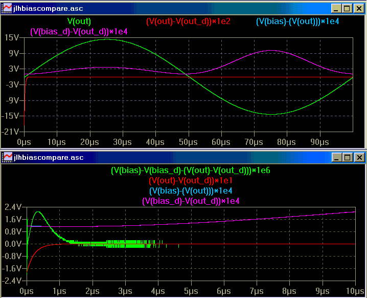
The top plot shows the difference between the normal jlh style output and current regulated bias circuit V(bias) in blue(= 2nd cycle, ~steady state) and purple(= 1st cycle) traces; at 10K gain you cannot see the difference in 1st and second cycle response – purple totally overlays blue
The second plot shows the 1st 10 uS, at this resolution a little blue can be seen under the purple in the 1st uS, blowing up the “difference of the differences” by a million (green) we can see the miniscule difference in the two circuits’ dynamic response - the 20 ppb “hair” on the green trace is spice numeric issues, not oscillation
The repeatable cyclic difference between the 2 circuits is solely the result of the intentional operation of the current regulator modulating the current at the base of Q3 to servo the Q3,4 output current sum; with finite loop gain and the added constraint of constant Q3,4 current the feedback loop does have to work harder to get the desired difference current output, that shows up as the V(out), V(bias) difference at -80 dB down
I clearly identified the cost in added distortion – this bias circuit does cause added distortion but not “1st cycle” distortion, the time domain dynamics of the current regulation loop are only loosely coupled to the main (differential output current) loop and do not change the dynamics of the jlh output stage – even with your 1st cycle test signal
My simplified circuit doesn’t include diff pair/mirror dynamics, but with the high bias and with reasonable small signal devices I assume there are no loop influencing poles below ~10 MHz and that should assure that even your “1st cycle” is unaffected in any meaningful way
Given the inaccuracies of the spice models and unmodeled pcb/packaging/wiring parasitics in addition to the simplified front end, ignoring 50+ MHz transients that quickly damp out seems reasonable for this APPROXIMATE model when we have the example of your real world circuit being well behaved; it is well behaved at these frequencies, right?
For a fair comparison of the current regulator idea within the context of your “1st cycle distortion” paradigm I’m comparing 1st cycle response with the 2nd cycle response with the current regulation the only difference in the circuits
I duplicated the “normal” and “current regulator biased” pair of circuits a second time and changed the 1 V 10 KHz sine Vin of the top pair to the same with the start delayed by 100 uS for the second “pair of pairs” – 4 amplifier circuits
1st pair (blown up, cropped 8 Ohm load R still in circuit; left output = V(out), right output = V(bias)):
I cranked LtSpice default simulation tol limits 2 orders of magnitude, and simulated with 1 nS max time step; .tran starts collecting data after the 1st 100 uS
Looking at the response from 100 to 200 uS I am comparing your 1st cycle response (V(out_d), _d for delayed sine input which starts at 100 uS) with the “2nd cycle” response V(out) which has had 100 US of 10KHz sine input to reach steady state
The top plot shows the difference between the normal jlh style output and current regulated bias circuit V(bias) in blue(= 2nd cycle, ~steady state) and purple(= 1st cycle) traces; at 10K gain you cannot see the difference in 1st and second cycle response – purple totally overlays blue
The second plot shows the 1st 10 uS, at this resolution a little blue can be seen under the purple in the 1st uS, blowing up the “difference of the differences” by a million (green) we can see the miniscule difference in the two circuits’ dynamic response - the 20 ppb “hair” on the green trace is spice numeric issues, not oscillation
The repeatable cyclic difference between the 2 circuits is solely the result of the intentional operation of the current regulator modulating the current at the base of Q3 to servo the Q3,4 output current sum; with finite loop gain and the added constraint of constant Q3,4 current the feedback loop does have to work harder to get the desired difference current output, that shows up as the V(out), V(bias) difference at -80 dB down
I clearly identified the cost in added distortion – this bias circuit does cause added distortion but not “1st cycle” distortion, the time domain dynamics of the current regulation loop are only loosely coupled to the main (differential output current) loop and do not change the dynamics of the jlh output stage – even with your 1st cycle test signal
Attachments
Hi jcx,
I am at a loss in seeing what you are trying to prove.
Again this appears to be steady sinewave testing, again without the full amplifier circuit, and again without a virtual loudspeaker load.
I would not run the tests that you are for they are not sufficiently representative of AUDIO amplifier usage.
Cheers ....... Graham.
you might try reading and thinking carefully Graham, heck maybe even download and run the sim yourself
the sim is the highest resolution "1st cycle" comparison i could think of not "steady sinewave testing"
it is not intended to be a full amplifier sim, i'm trying to illustrate the operation of a simple circuit modification in the least complex circuit environment that will show up the operating principles and major performance issues
i feel i am going some distance to try to present this comparison in your "1st cycle" paradigm
if you have some specific suggestions about what level of sim is required to "prove" anything we can explore them next week
Hi jcx,
Well, it has now come to you assuming that I need to brush up on my reading !!!
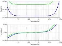
Please find enclosed the simulated output impedance characteristics for my amp in blue, as well as with your bias network fitted in green. Do these characteristics match yours ?
( I ran 50mA and 5mA current sources for your arrangement. )
Your biasing network is the only difference between these two traces.
The effect of steady sinewave amplifier-loudspeaker interface amplitude distortion caused by loudspeaker induced back EMF upon amplifier output can be calculated from the numerical figure from the dB-damping figure, multiplied by the numerical Sine figure for the degrees of shift at the frequency of examination.
Illustrated are differences of between 3.5dB and zero degrees @ 200Hz, and 64.2 to 60dB and 16 to 24.5 degrees @ 20kHz. Thus your suggested biasing network increases loudspeaker induced distortion between factors of 1.5 at 200Hz and 2.4 at 20kHz, and this would contraindicate its usage where optimum treble clarity from the simple JLH output stage is required.
* This has nothing to do with forward simulated and measured sinewave distortion, nor prime frequency ratios !!! *
Can you not see that your bias control transistor works wrt the slow lower output transistor collector. In a JLH proper the bias is controlled by the much faster driver transistor. This is why the driver transistor needs to be fast, for a driver that is slow will increase phase change with a possible risk of instability as well as reduced clarity of treble reproduction. Similarly, outputs that are almost as fast as the driver could oscillate; this is why I use the lower impedance Zobel, without any need for stabilising capacitors.
If you want to observe the first cycle or steady sinewave distortions that arise due to loudspeaker loading an amplifier as loudspeaker crossover network capacitors momentarily behave like short circuits to audio transients and inductors build up their magnetic fields before passing current you need to simulate with a virtual loudspeaker load, plus fundamental null the output.
The dB damping figures for original JLH designs tend to be circa 30-40dB, and this is mirrored by the substantial improvement in high frequency reproduction clarity with my 25W design, with its increased open loop gain / NFB.
jcx, I believe you mentioned an increase in NFB for your biasing arrangement but I cannot go back to check your posts without losing this window. I find only a reduction in NFB and thus a degradation in performance.
Are you trying to make some other point that I am not aware of ?
Cheers .............. Graham.
Well, it has now come to you assuming that I need to brush up on my reading !!!
Please find enclosed the simulated output impedance characteristics for my amp in blue, as well as with your bias network fitted in green. Do these characteristics match yours ?
( I ran 50mA and 5mA current sources for your arrangement. )
Your biasing network is the only difference between these two traces.
The effect of steady sinewave amplifier-loudspeaker interface amplitude distortion caused by loudspeaker induced back EMF upon amplifier output can be calculated from the numerical figure from the dB-damping figure, multiplied by the numerical Sine figure for the degrees of shift at the frequency of examination.
Illustrated are differences of between 3.5dB and zero degrees @ 200Hz, and 64.2 to 60dB and 16 to 24.5 degrees @ 20kHz. Thus your suggested biasing network increases loudspeaker induced distortion between factors of 1.5 at 200Hz and 2.4 at 20kHz, and this would contraindicate its usage where optimum treble clarity from the simple JLH output stage is required.
* This has nothing to do with forward simulated and measured sinewave distortion, nor prime frequency ratios !!! *
Can you not see that your bias control transistor works wrt the slow lower output transistor collector. In a JLH proper the bias is controlled by the much faster driver transistor. This is why the driver transistor needs to be fast, for a driver that is slow will increase phase change with a possible risk of instability as well as reduced clarity of treble reproduction. Similarly, outputs that are almost as fast as the driver could oscillate; this is why I use the lower impedance Zobel, without any need for stabilising capacitors.
If you want to observe the first cycle or steady sinewave distortions that arise due to loudspeaker loading an amplifier as loudspeaker crossover network capacitors momentarily behave like short circuits to audio transients and inductors build up their magnetic fields before passing current you need to simulate with a virtual loudspeaker load, plus fundamental null the output.
The dB damping figures for original JLH designs tend to be circa 30-40dB, and this is mirrored by the substantial improvement in high frequency reproduction clarity with my 25W design, with its increased open loop gain / NFB.
jcx, I believe you mentioned an increase in NFB for your biasing arrangement but I cannot go back to check your posts without losing this window. I find only a reduction in NFB and thus a degradation in performance.
Are you trying to make some other point that I am not aware of ?
Cheers .............. Graham.
Attachments
summary of dialog
Hello Graham, and others,
Thanks for sharing the insights and proceedings of the JLHood-heritage in this thread and in the series in Electronics World.
I'm trying to unterstand this very interesting thread with my limited EE-education. It would be helpfull if someone could summerise the findings of the dialog so far; does it lead us anywhere?
Also, I'm interested in 'diy-ing' the GM-25/8 myself. I'm listening to the 1969-asymetrical JLH-version still frequently with pleasure.
I've noticed the photo's here of some-one that apparently made a pcb-design. Is this design available (or may be even a ready-pcb)? It would save lots of time for those who want to build it.
Best regards, Arjen.
Hi Arjen,
I very much prefer that individuals draw their own conclusions, rather than examine a concensus, for then there is less chance of ideological or theoretical entrapment.
The JLH amplifiers (and mine) are two stage and have a naturally good open loop af frequency response. With careful construction and device selection, stability does not need to be forced upon them by connecting tiny 'C.doms', which, with class-B output stages can lead to distorted high audio frequency dynamics when the loudspeakers generate back EMFs.
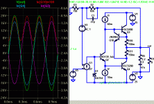
John Lui was the first to construct my 25W amplifier from scratch; he kindly forwarded me a photo of his pcb which is shown here.
He has implemented an excellent star earth, but has the Zobel components close to the input transistors. JLH type amplifiers have gain into the low short-wave frequencies, and thus output-input wiring separation is as essential as it is with a radio frequency stage; thus I would recommend that Zobel components are always spaced on the pcb.
I will forward my own hand-drawn (amateur but entirely functional) stripboard layout to anyone who requests it from me via
graham.maynard1@virgin.net
Cheers ............. Graham.
I very much prefer that individuals draw their own conclusions, rather than examine a concensus, for then there is less chance of ideological or theoretical entrapment.
The JLH amplifiers (and mine) are two stage and have a naturally good open loop af frequency response. With careful construction and device selection, stability does not need to be forced upon them by connecting tiny 'C.doms', which, with class-B output stages can lead to distorted high audio frequency dynamics when the loudspeakers generate back EMFs.
John Lui was the first to construct my 25W amplifier from scratch; he kindly forwarded me a photo of his pcb which is shown here.
He has implemented an excellent star earth, but has the Zobel components close to the input transistors. JLH type amplifiers have gain into the low short-wave frequencies, and thus output-input wiring separation is as essential as it is with a radio frequency stage; thus I would recommend that Zobel components are always spaced on the pcb.
I will forward my own hand-drawn (amateur but entirely functional) stripboard layout to anyone who requests it from me via
graham.maynard1@virgin.net
Cheers ............. Graham.
Attachments
Graham, when you completely missed the point of my previous post it seemed reasonable to point out that it said something different – if I didn’t succeed in communicating then asking for clarification rather than posting a hasty dismissal would be more useful
You still seem to be making comparisons of my posted simplified test circuit and your own complete amplifier model which is apparently different in several regards – the only fair test of the bias circuit is in otherwise identical circuits operating with the same bias currents in driver and output transistors
When I take a few min to edit the test sources appropriately for 1 A current sources across the outputs and run a AC sweep on my posted test circuit I find only 0.2 dB, 0.36 degree diff @20 KHz; 0.34 dB, 3.3 degree @200 KHz and a max diff of 1.9 dB @2 MHz in the simulated output impedance
Since output impedance is determined by loop gain any difference that changes loop gain changes output impedance, a few quick driver transistor model substitutions easily caused 2-6 dB diff in the output Z in my test sim
thanx for your continued engagement despite our communication difficulties
john
Hi John,
This is the comparison circuit I used. Your output stage has higher output current, but higher instead of lower output impedance.
Yes device gain alters output impedance, but it makes hardly any change on forward measured amplitude and frequency response etc.
Cheers ........... Graham.
This is the comparison circuit I used. Your output stage has higher output current, but higher instead of lower output impedance.
Yes device gain alters output impedance, but it makes hardly any change on forward measured amplitude and frequency response etc.
Cheers ........... Graham.
Attachments
Congratulations Mr. Graham Maynard, your amplifier is wonderfull
Please, let me receive the text published with your amplifier.
My friends and I, we had a meeting today, i gonne with three amplifiers to be compared.
Your amplifier sound magnificent.
Please send me your picture, will go to our Club, if signed picture is better,
thanks in advance your kindness,
honored with your attention
Carlos
- Status
- This old topic is closed. If you want to reopen this topic, contact a moderator using the "Report Post" button.
- Home
- Amplifiers
- Solid State
- Graham's Class A/JLH output