audioDIYer said:As I said before
Blue or grey smoke?... Let's bet
This extends to AndrewT and peranders
before i turn on the amp, i will call the fire dept!
another PCB for laterals ......
Hi,
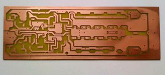
Another PCB variant , corrected for laterals http://i34.tinypic.com/t4tkso.gif regards alex mm
Hi,
Another PCB variant , corrected for laterals
http://i34.tinypic.com/t4tkso.gif regards alex mm

Attachments
AndrewT said:and still no sign of the Source resistors
I think he has changed his mind and is going to use BUZ901P which are laterals. Then it will work without source resistors.
But why do a quasi complementary lateral design, I can't understand the reason for that...

One of the schematics earlier had some transistors that had the wrong polarity but part number was right. Upper vas transistor was a BC556 but drawn as an NPN for example
Watch out!netuddki said:
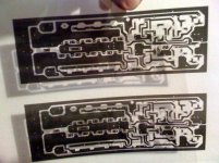
NO! I'am using a film!
Photographic film?
We have some nice equipment at school for making PCB:s, with a camera similar to this but not as modern:
http://www.photoandi.com/UserFiles/Image/Repro-Camera.jpg
The film we use is negative and the photo-resist is so that it protects copper where it was exposed to light, the film is transparent where you want copper to stay. This means you can put your standard black copper trace layouts in the camera (preferably in 200% size for better printer resolution).
Exposure time is about 30 seconds, both for films in the camera and boards in the double sided UV machine.
There are two huge machines for developing and etching the PCB:s. You start the pump and motor and put in the board on one end of the machine and it comes out the other end, rinsed and everything!!
megajocke said:
One of the schematics earlier had some transistors that had the wrong polarity but part number was right. Upper vas transistor was a BC556 but drawn as an NPN for example
Mega you might just have saved Netuddki from some blue smoke.

- Status
- This old topic is closed. If you want to reopen this topic, contact a moderator using the "Report Post" button.
- Home
- Amplifiers
- Solid State
- from the net