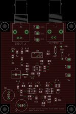
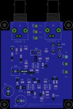
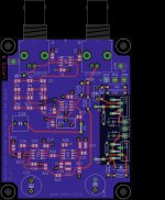
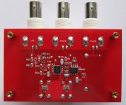
Dual chip board for the AD8397
I sent this one out to fabrication yesterday, a small dual op-amp Fliege notch filter test board. I've left the power supply off this one since the odds are it will probably oscillate with anything other than the THS4032.
Curiousity just has the better of me if the AD8397 is going to work in the Fliege notch filter.") The chip seems so similar to the THS4031/2 there may be a chance, without further circuit tinkering. The AD8397 is also apparently a high current line driver with a fairly high GBW and slew rate. The slew looks to be about twice that of the LME49990 & OPA1611. The triangular shape of the oscillation has me wondering if slew might be a factor.
The chip seems so similar to the THS4031/2 there may be a chance, without further circuit tinkering. The AD8397 is also apparently a high current line driver with a fairly high GBW and slew rate. The slew looks to be about twice that of the LME49990 & OPA1611. The triangular shape of the oscillation has me wondering if slew might be a factor.
After yet a few more re-readings of the TI Fliege notch filter white paper here
www.ti.com/lit/an/slyt235/slyt235.pdf
I'm back to thinking the higher op-amp GBW *is* needed after all. The TI author contradicts himself in the sheet. Early on he gives the rule of thumb of the GBW being 100x the notch frequency. But then later in the paper, when they are actually testing it, they find that "100MHz GBW [the THS4032 chip] is the minimum for a 10KHz - 100KHz notch" based on their measured notch quality. That works out to be a factor of 1,000x - 10,000x between notch frequency and GBW, not 100. For an 11KHz notch that would be a minimum of 11MHz, so the AD8397 might fit the bill there too.
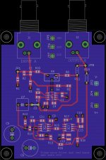
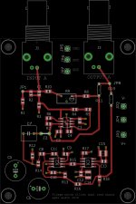
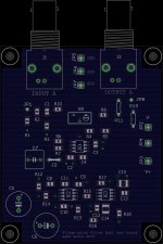
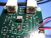
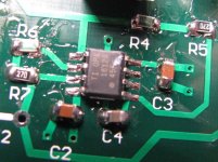
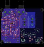
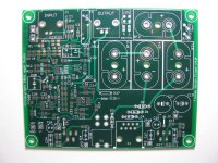
I've used some of marce's tips in the layout. The ground and power plane notch-outs are gone. I've put the 7mm circles around the mounting screw holes to mark for nut clearance. The parts are all 0805 now so the spacings on all the loops and traces have decreased. I've left the traces under the chips.
Now if I can just remember to reduce the power supply voltage to +/-12Vdc from the +/-15.3Vdc when testing before I fry the thing.
I sent this one out to fabrication yesterday, a small dual op-amp Fliege notch filter test board. I've left the power supply off this one since the odds are it will probably oscillate with anything other than the THS4032.
Curiousity just has the better of me if the AD8397 is going to work in the Fliege notch filter.
The chip seems so similar to the THS4031/2 there may be a chance, without further circuit tinkering. The AD8397 is also apparently a high current line driver with a fairly high GBW and slew rate. The slew looks to be about twice that of the LME49990 & OPA1611. The triangular shape of the oscillation has me wondering if slew might be a factor.After yet a few more re-readings of the TI Fliege notch filter white paper here
www.ti.com/lit/an/slyt235/slyt235.pdf
I'm back to thinking the higher op-amp GBW *is* needed after all. The TI author contradicts himself in the sheet. Early on he gives the rule of thumb of the GBW being 100x the notch frequency. But then later in the paper, when they are actually testing it, they find that "100MHz GBW [the THS4032 chip] is the minimum for a 10KHz - 100KHz notch" based on their measured notch quality. That works out to be a factor of 1,000x - 10,000x between notch frequency and GBW, not 100. For an 11KHz notch that would be a minimum of 11MHz, so the AD8397 might fit the bill there too.
I've used some of marce's tips in the layout.
The ground and power plane notch-outs are gone. I've put the 7mm circles around the mounting screw holes to mark for nut clearance. The parts are all 0805 now so the spacings on all the loops and traces have decreased. I've left the traces under the chips.Now if I can just remember to reduce the power supply voltage to +/-12Vdc from the +/-15.3Vdc when testing before I fry the thing.
Attachments
-
 schematic.jpg394.8 KB · Views: 485
 -
schematic.pdf23.3 KB · Views: 119
-
 layout.jpg886.3 KB · Views: 422
 -
 layer 1 route.jpg386.3 KB · Views: 382
 -
 layer 2 ground.jpg969 KB · Views: 361
 -
 layer 3 V+.jpg947 KB · Views: 357
 -
 layer 4 V-.jpg392.6 KB · Views: 96
 -
layout.pdf170.1 KB · Views: 67
-
Fliege notch dual chip BOM 3.zip16.2 KB · Views: 66
Last edited:
Twin-T PCB layout for the QuantAsylum blog post
I've whipped up a PCB that matches the 1KHz Twin-T in the QuantAsylum blog post that dontbugme pointed out:
Using Notch Filters to Improve THD Measurements - QuantAsylum
Given that QA has shown great looking (low) distortion results in that post with the twin-T, using the OPA1612 chips, it will be a useful fall-back if I can't get the Fliege notch filter to match that low distortion level.
I started with the values QA used, but I've made it a bit more accurate by putting 115R resistors in series with the 15.8K's. With just the 15.8Ks the notch is at 1007 Hz. With the 115's it should be at 1000.3 Hz, plus or minus part tolerances. The part numbers are on the schematic again (sorry marce! didn't want to take the time to make a BOM). The resistors are all 0.1%, most at 10PPM/C, and the caps are C0G 1%.
There is a single OPA1611 for the input op amp, then a dual OPA1612 for the filter. I built this starting with the same Fleige notch board I have in for fab right now, so I left the post-amplifier circuit. Works the same way. The twin-T output can be run directly to the output BNC via an optional (49.9R) series resistor. Or by changing the resistors and jumpers the output of the twin-T can be fed through the post-amplifier, then that to the output BNC.
The power supply is optional to populate. Run regulated +/-15Vdc directly into JP4, JP5, and JP6 but leave off the power disconnects J2 and J3 (and don't populate the power supply parts). OR leave JP4, JP5, and JP6 open, connect J2 and j3 (jumpers), then feed the unregulated voltage into JP2, JP3, and JP8.
I hadn't look at the twin-T in a couple of years. I remember why I didn't like it now. No easy way to fine tune the notch to compensate for those 1% capacitors. Three resistors would have to be varied at once, vs just the one nice trimpot on the Fliege. In doing some net research for this I see folks have used switches in some designs to switch those 3 resistors in and out. With the Fliege notch filter I can easily adjust the frequency fine-tuning trimpot on either side of the notch bottom. I'll take the Fliege notch filter over the twin-T any day if I can get one together with acceptably low distortion.
I was going to put this in a different thread but I was able to modify the title to include the twin-T. I'll probably fabricate this board at some point, just to compare with the Fliege. If I do fab it I'll post the Gerbers if it works.
I've whipped up a PCB that matches the 1KHz Twin-T in the QuantAsylum blog post that dontbugme pointed out:
Using Notch Filters to Improve THD Measurements - QuantAsylum
Given that QA has shown great looking (low) distortion results in that post with the twin-T, using the OPA1612 chips, it will be a useful fall-back if I can't get the Fliege notch filter to match that low distortion level.
I started with the values QA used, but I've made it a bit more accurate by putting 115R resistors in series with the 15.8K's. With just the 15.8Ks the notch is at 1007 Hz. With the 115's it should be at 1000.3 Hz, plus or minus part tolerances. The part numbers are on the schematic again (sorry marce! didn't want to take the time to make a BOM). The resistors are all 0.1%, most at 10PPM/C, and the caps are C0G 1%.
There is a single OPA1611 for the input op amp, then a dual OPA1612 for the filter. I built this starting with the same Fleige notch board I have in for fab right now, so I left the post-amplifier circuit. Works the same way. The twin-T output can be run directly to the output BNC via an optional (49.9R) series resistor. Or by changing the resistors and jumpers the output of the twin-T can be fed through the post-amplifier, then that to the output BNC.
The power supply is optional to populate. Run regulated +/-15Vdc directly into JP4, JP5, and JP6 but leave off the power disconnects J2 and J3 (and don't populate the power supply parts). OR leave JP4, JP5, and JP6 open, connect J2 and j3 (jumpers), then feed the unregulated voltage into JP2, JP3, and JP8.
I hadn't look at the twin-T in a couple of years. I remember why I didn't like it now.
No easy way to fine tune the notch to compensate for those 1% capacitors. Three resistors would have to be varied at once, vs just the one nice trimpot on the Fliege. In doing some net research for this I see folks have used switches in some designs to switch those 3 resistors in and out. With the Fliege notch filter I can easily adjust the frequency fine-tuning trimpot on either side of the notch bottom. I'll take the Fliege notch filter over the twin-T any day if I can get one together with acceptably low distortion.I was going to put this in a different thread but I was able to modify the title to include the twin-T. I'll probably fabricate this board at some point, just to compare with the Fliege. If I do fab it I'll post the Gerbers if it works.
Attachments
Last edited:
AD8397 works fine but needs a lower rail voltage
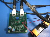
The dual op-amp boards I sent out to fabrication came back already! The AD8397 dual op-amp does indeed work just fine in the Fliege notch filter circuit, but there is a trick. +/-12Vdc power rails will cause thermal runaway in about 2 minutes. Going to a lower rail voltage solves the problem.
After starting off with +/-12Vdc power rails I wound up with just two 9V batteries hardwired in, at measured voltages of about 8.2Vdc each. Completely stable and the notch bottom does appear deeper than with the THS4031 chips in the V3.0 board.
I have a lot more testing to do, but the AD8397 does appear to be a viable alternative to the THS4031/2.
Details....
When I first tested it with a +/-12V feed from the V3.0 board the output looked just great. No oscillation and the notch was working quite well by vaying the signal generator, other than the notch wound up at 994Hz instead of 1.000. Probably part tolerances but I'm still looking into that one.
But then after about two minutes the filter output waveform suddenly zoomed off the bottom of the scope screen. Doing some troubleshooting I discovered that the output DC offset (measured at the board output BNC connector) started at zero, but then very slowly went negative, speeding up the rate with time, until at the two minute or so point it hit the negative rail. At that point I had to go back and measure the V3.0 board with the single op-amps (THS4031) to make sure it wasn't doing that, and it wasn't. This output DC offset shift was something unique to the AD8397.
Turning the power off for a minute and back on would reset the thing and the DC offset rise from 0Vdc would start again. I didn't have to think very hard to figure out the problem on this one. I remember the various discussion posts years ago on Headwize when AMB and Morsel were designing the mini^3 headamp with the AD8397. I recall a consensus back then that the chip didn't really run on +/-12Vdc, despite what the data sheet says, and they decided to use a lower voltage. Looking at the sheet you will find identical specification tables for +/-1.5Vdc, +/-2.5Vdc, +/-5Vdc, then it jumps up to one for +/-12Vdc. I would imagine the chip was designed for +/-5Vdc but the process just happened to go up to 12Vdc or so.
In fairness to AD the chip did turn out to be a power pad with the metal heat sink pad on the bottom. I didn't include the proper heat sink foil area & vias under the chip. That may have helped, or even prevented the problem. But I really don't think its a package dissipation issue. I used technical freeze spray on the chip and it made no difference. The output loading in this circuit is also well within what should be safe operating area. I think it is just a case of some internal junctions exceeding 150C at +/-12Vdc over time, regardless of package cooling. I believe the chip simply doesn't work properly at +/-12Vdc rails.
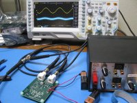
But at 8.2Vdc rails all is good. I just hard wired in the batteries as a test of the theory before changing the votlage regulator output on the V3.0 board again, or digging out one of the 30lb lab supplies. Works just fine on +/-8.2Vdc
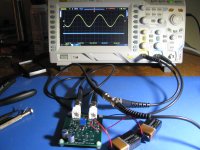
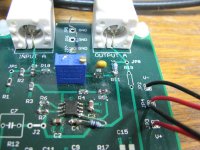
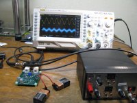
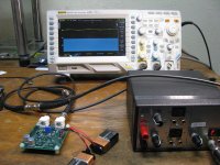
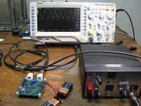
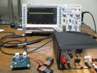
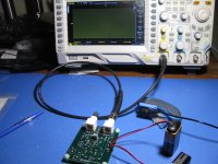
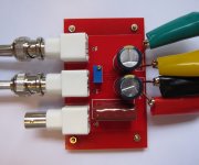
Photos -
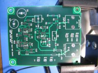
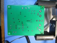
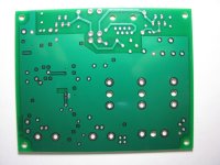
* 3888 and 3889 are the front and back of the bare board. No notched-out areas in the ground or power planes this time, thanks to marce's suggestion.
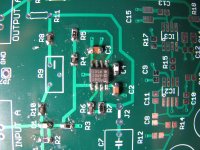
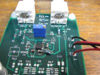
* The next two are the SMD stuff soldered on, then the through hole parts. I didn't build up the post-filter-amp below for this test, just ran the notch filter output to the BNC via a 49.9R resistor.
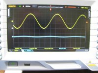
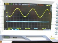
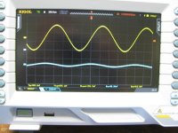
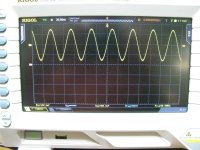
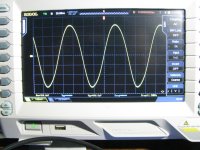
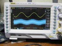
* The next one is the test setup. Blue trace is the output and yellow the input from the signal generator. The scope in the background is showing the (blue) notch bottom result with the input at 994Hz.
* The next two are 6Hz either way from the notch bottom, 1.000KHZ and 988Hz. Just showing here that the notch filter is in fact a notch filter.
* The next is 10Hz away from the notch, 1004Hz
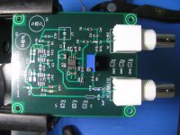
* The final one is a closeup of the hardwired 9V cells.
It has occured to me recently that most of the noise I'm seeing when looking at the notch bottom at high scope gain isn't the scope or even EMI into the notch filter board, but the signal generator. When I unplug the signal generator from the notch filter board input BNC all the noise goes away. I'm going to try that notch-bottom test again with the V3.0 single op amp board using Victor's low noise single frequency oscillator and see if the result is a cleaner signal.
The dual op-amp boards I sent out to fabrication came back already! The AD8397 dual op-amp does indeed work just fine in the Fliege notch filter circuit, but there is a trick. +/-12Vdc power rails will cause thermal runaway in about 2 minutes. Going to a lower rail voltage solves the problem.
After starting off with +/-12Vdc power rails I wound up with just two 9V batteries hardwired in, at measured voltages of about 8.2Vdc each. Completely stable and the notch bottom does appear deeper than with the THS4031 chips in the V3.0 board.
I have a lot more testing to do, but the AD8397 does appear to be a viable alternative to the THS4031/2.
Details....
When I first tested it with a +/-12V feed from the V3.0 board the output looked just great. No oscillation and the notch was working quite well by vaying the signal generator, other than the notch wound up at 994Hz instead of 1.000. Probably part tolerances but I'm still looking into that one.
But then after about two minutes the filter output waveform suddenly zoomed off the bottom of the scope screen. Doing some troubleshooting I discovered that the output DC offset (measured at the board output BNC connector) started at zero, but then very slowly went negative, speeding up the rate with time, until at the two minute or so point it hit the negative rail. At that point I had to go back and measure the V3.0 board with the single op-amps (THS4031) to make sure it wasn't doing that, and it wasn't. This output DC offset shift was something unique to the AD8397.
Turning the power off for a minute and back on would reset the thing and the DC offset rise from 0Vdc would start again. I didn't have to think very hard to figure out the problem on this one. I remember the various discussion posts years ago on Headwize when AMB and Morsel were designing the mini^3 headamp with the AD8397. I recall a consensus back then that the chip didn't really run on +/-12Vdc, despite what the data sheet says, and they decided to use a lower voltage. Looking at the sheet you will find identical specification tables for +/-1.5Vdc, +/-2.5Vdc, +/-5Vdc, then it jumps up to one for +/-12Vdc.
I would imagine the chip was designed for +/-5Vdc but the process just happened to go up to 12Vdc or so.In fairness to AD the chip did turn out to be a power pad with the metal heat sink pad on the bottom. I didn't include the proper heat sink foil area & vias under the chip. That may have helped, or even prevented the problem. But I really don't think its a package dissipation issue. I used technical freeze spray on the chip and it made no difference. The output loading in this circuit is also well within what should be safe operating area. I think it is just a case of some internal junctions exceeding 150C at +/-12Vdc over time, regardless of package cooling. I believe the chip simply doesn't work properly at +/-12Vdc rails.
But at 8.2Vdc rails all is good. I just hard wired in the batteries as a test of the theory before changing the votlage regulator output on the V3.0 board again, or digging out one of the 30lb lab supplies.
Works just fine on +/-8.2VdcPhotos -
* 3888 and 3889 are the front and back of the bare board. No notched-out areas in the ground or power planes this time, thanks to marce's suggestion.
* The next two are the SMD stuff soldered on, then the through hole parts. I didn't build up the post-filter-amp below for this test, just ran the notch filter output to the BNC via a 49.9R resistor.
* The next one is the test setup. Blue trace is the output and yellow the input from the signal generator. The scope in the background is showing the (blue) notch bottom result with the input at 994Hz.
* The next two are 6Hz either way from the notch bottom, 1.000KHZ and 988Hz. Just showing here that the notch filter is in fact a notch filter.
* The next is 10Hz away from the notch, 1004Hz
* The final one is a closeup of the hardwired 9V cells.
It has occured to me recently that most of the noise I'm seeing when looking at the notch bottom at high scope gain isn't the scope or even EMI into the notch filter board, but the signal generator. When I unplug the signal generator from the notch filter board input BNC all the noise goes away. I'm going to try that notch-bottom test again with the V3.0 single op amp board using Victor's low noise single frequency oscillator and see if the result is a cleaner signal.
Attachments
-
 IMG_3988.JPG229.9 KB · Views: 106
 -
 IMG_3989.JPG159.2 KB · Views: 85
 -
 IMG_3992.JPG277.3 KB · Views: 92
 -
 IMG_3993.JPG211.2 KB · Views: 96
 -
 IMG_3995.JPG220.2 KB · Views: 92
 -
 IMG_3998.JPG150.2 KB · Views: 93
 -
 IMG_3999.JPG157 KB · Views: 69
 -
 IMG_4000.JPG163.5 KB · Views: 76
 -
 IMG_4001.JPG260.2 KB · Views: 102
Last edited:
AD8397A notch frequency shift solved, notch around -54dB.
After experimenting with a couple of different builds of the AD8397A based Fliege notch filter, I believe that I've figured out the source of a meaured 6Hz notch shift from the calculated value. A related problem was that the 10R trimpot I've used successfully on the single op-amp THS4031 V3.0 boards for frequency fine-tuning had very little effect. With the V3.0 board using single THS4031 op-amps the measured frequency was an exact match to the calculated value (1.000KHz).
The problem appears to be around 150pF of input-to-output capacitance, or at least a circuit that "looks" capacitive from the outside, inside the AD8397A chip from output to inverting input. The extra 150pF winds up in parallel with one of the Fliege notch "frequency set" capacitors, which is enough to shift the 1.000KHz notch down 6Hz to the measured 994Hz. The 10R trimpot was designed to adjust +/-1% to compensate for the 1% tolerance of the capacitors. It didn't have anywhere near enough range to adjust for 6%, hence the reason the pot did very little here, even though the same value worked fine on the V3.0 board with the THS4031's.
My first "fix" was simply increasing the value of the frequency fine-tune trimpot to 200R, which worked great. 100R was not quite enough to scan through the notch frequency.
After that worked I went back and reduced the 84.5R "frequency set" resistors to 49.9R to bump the notch frequency up 6Hz to compensate for the capacitance in the chip. That also worked. With the change I was able to drop the trimpot back down to 50R.
I've built up two different AD8397A Fliege notch filter boards with two different pairs of frequency-set capacitors and resistors that both produce a notch at 1KHz. I was just curious if the different equivalent values altered the notch depth with the AD8397A even though they both produced a 1KHz notch. They did!
One board used 0.047uF (C0G, 1%) caps with a 3.36K+27R resistor pair (0.1%), and a 33K Qset resistor for Q=5. This combination is what I used in the V3.0 board with the THS4031 op amps. The other board used 0.022uF (COG, 1%) and a 7.15K+84.5R resistor pair (0.1%) with a 71.5K Qset (Q=5 again).
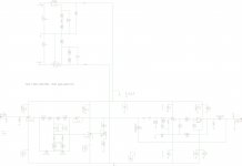
Again for reference on the Fliege circuit and schematic see the TI paper here (figure 4)
http://www.ti.com/lit/an/slyt235/slyt235.pdf (opens PDF)
The best notch with the 0.022uf set was 2mVp-p. With the 0.047uF set I was able to go down to 1mVp-p. This more-or-less matches simulation results. 0.047uf + 3.36K produces a deeper simulated notch than 0.022uF + 7.15K, and that produces a deeper notch than 0.01uF + 15.8K (the values that TI used in their paper). 0.047uF is the biggest standard C0G value available now, but I assume two could be put in parallel, with a 1.68K frequency set resistor, for an even deeper notch, if the particular op amp can drive 1.68K at low distortion levels.
The reason the bigger capacitors produce deeper notches is probably the value of the impedance of the cap being lower at the notch frequency. At the notch frequency the impedance of the Fliege notch frequency "set" capacitors equal the resistance of the frequency set resistors. So the Z of the 0.047uF capacitor is 3.36K (plus phase shift) at 1KHz, matching the 3.36K "set" resistors. Lower impedance/resistor values probably result in higher feedback levels, resulting in the deeper notches.
I also whipped out the Victor low noise oscillators as an input source, which did significantly reduce the output noise.
The best notch I was able to get was -54db, which is right around what the V3.0 board with the two single THS4031s was measured at. I guess it will come down to which one has the fewest additional distortion products when viewed with a Q400 or 401.
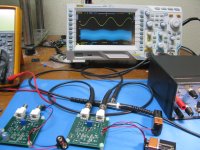
Photos:
* The first shows the test setup. The board on the left is the 0.022uF + (7.15K + 85.5R) AD8397A Fliege notch board. The board on the right is the 0.047uF + (3.36K + 27R) board. The (shielded!) box on the right is Victor low THD+N oscillators, 1KHz, 10KHz, and 11KHz. On the scope the top trace is the 1KHz oscillator going into the Fliege notch board at 500mVp-p, with the scope on 200mV/div. The bottom blue trace is the output of the Fliege notch filter with the trimpot tuned for the best notch. About 1mVp-p of actual signal in the noise, with the scope on 1mV/div here. -54dB.
* The next two show a 10KHz input signal, just to see what happens far away from the notch frequency. As expected the output matches the input amplitude and phase.
* The final one is a bit of noise analysis. I've removed the input BNC cable which shows about 2mV of noise on the scope. But unplugging the input at the scope shows about 0.75mV of noise just in the scope's vertical amplifier. So the notch filter is generating about 1mV of noise, but it is unshielded here too. Note that I've expanded the time base way out on the scope to get a better look at the noise (blue) signal. Nothing sinusoidal or periodic, no oscillation. Just random noise.
So here is an observation about the Fliege notch filter. The detailed properties of the op-amps wind up much more part of the tuned circuit than with the Twin-T, such as the (likely) 150pF internal input-to-output capacitance here with the AD8397A. For awhile I was also suspecting a low AD8397A input resistance, since the AD8397A data sheet lists Rin=87K with no further details. But after some testing that must be differential (input to input) resistance rather than common mode (input to ground), since a low op-amp input resistance would actually cause the notch frequency to go up rather than down.
After experimenting with a couple of different builds of the AD8397A based Fliege notch filter, I believe that I've figured out the source of a meaured 6Hz notch shift from the calculated value. A related problem was that the 10R trimpot I've used successfully on the single op-amp THS4031 V3.0 boards for frequency fine-tuning had very little effect. With the V3.0 board using single THS4031 op-amps the measured frequency was an exact match to the calculated value (1.000KHz).
The problem appears to be around 150pF of input-to-output capacitance, or at least a circuit that "looks" capacitive from the outside, inside the AD8397A chip from output to inverting input. The extra 150pF winds up in parallel with one of the Fliege notch "frequency set" capacitors, which is enough to shift the 1.000KHz notch down 6Hz to the measured 994Hz. The 10R trimpot was designed to adjust +/-1% to compensate for the 1% tolerance of the capacitors. It didn't have anywhere near enough range to adjust for 6%, hence the reason the pot did very little here, even though the same value worked fine on the V3.0 board with the THS4031's.
My first "fix" was simply increasing the value of the frequency fine-tune trimpot to 200R, which worked great. 100R was not quite enough to scan through the notch frequency.
After that worked I went back and reduced the 84.5R "frequency set" resistors to 49.9R to bump the notch frequency up 6Hz to compensate for the capacitance in the chip. That also worked. With the change I was able to drop the trimpot back down to 50R.
I've built up two different AD8397A Fliege notch filter boards with two different pairs of frequency-set capacitors and resistors that both produce a notch at 1KHz. I was just curious if the different equivalent values altered the notch depth with the AD8397A even though they both produced a 1KHz notch. They did!
One board used 0.047uF (C0G, 1%) caps with a 3.36K+27R resistor pair (0.1%), and a 33K Qset resistor for Q=5. This combination is what I used in the V3.0 board with the THS4031 op amps. The other board used 0.022uF (COG, 1%) and a 7.15K+84.5R resistor pair (0.1%) with a 71.5K Qset (Q=5 again).
Again for reference on the Fliege circuit and schematic see the TI paper here (figure 4)
http://www.ti.com/lit/an/slyt235/slyt235.pdf (opens PDF)
The best notch with the 0.022uf set was 2mVp-p. With the 0.047uF set I was able to go down to 1mVp-p. This more-or-less matches simulation results. 0.047uf + 3.36K produces a deeper simulated notch than 0.022uF + 7.15K, and that produces a deeper notch than 0.01uF + 15.8K (the values that TI used in their paper). 0.047uF is the biggest standard C0G value available now, but I assume two could be put in parallel, with a 1.68K frequency set resistor, for an even deeper notch, if the particular op amp can drive 1.68K at low distortion levels.
The reason the bigger capacitors produce deeper notches is probably the value of the impedance of the cap being lower at the notch frequency. At the notch frequency the impedance of the Fliege notch frequency "set" capacitors equal the resistance of the frequency set resistors. So the Z of the 0.047uF capacitor is 3.36K (plus phase shift) at 1KHz, matching the 3.36K "set" resistors. Lower impedance/resistor values probably result in higher feedback levels, resulting in the deeper notches.
I also whipped out the Victor low noise oscillators as an input source, which did significantly reduce the output noise.
The best notch I was able to get was -54db, which is right around what the V3.0 board with the two single THS4031s was measured at. I guess it will come down to which one has the fewest additional distortion products when viewed with a Q400 or 401.
Photos:
* The first shows the test setup. The board on the left is the 0.022uF + (7.15K + 85.5R) AD8397A Fliege notch board. The board on the right is the 0.047uF + (3.36K + 27R) board. The (shielded!) box on the right is Victor low THD+N oscillators, 1KHz, 10KHz, and 11KHz. On the scope the top trace is the 1KHz oscillator going into the Fliege notch board at 500mVp-p, with the scope on 200mV/div. The bottom blue trace is the output of the Fliege notch filter with the trimpot tuned for the best notch. About 1mVp-p of actual signal in the noise, with the scope on 1mV/div here. -54dB.
* The next two show a 10KHz input signal, just to see what happens far away from the notch frequency. As expected the output matches the input amplitude and phase.
* The final one is a bit of noise analysis. I've removed the input BNC cable which shows about 2mV of noise on the scope. But unplugging the input at the scope shows about 0.75mV of noise just in the scope's vertical amplifier. So the notch filter is generating about 1mV of noise, but it is unshielded here too. Note that I've expanded the time base way out on the scope to get a better look at the noise (blue) signal. Nothing sinusoidal or periodic, no oscillation. Just random noise.
So here is an observation about the Fliege notch filter. The detailed properties of the op-amps wind up much more part of the tuned circuit than with the Twin-T, such as the (likely) 150pF internal input-to-output capacitance here with the AD8397A. For awhile I was also suspecting a low AD8397A input resistance, since the AD8397A data sheet lists Rin=87K with no further details. But after some testing that must be differential (input to input) resistance rather than common mode (input to ground), since a low op-amp input resistance would actually cause the notch frequency to go up rather than down.
Attachments
Last edited:
An oscillation cause & solution found
My dual-op amp Fliege notch filter board has worked reasonably well with the AD8397 per the posts above. But the THS4032 oscillated in the board, which has been especially curious since the THS4031 worked just fine with no oscillation in the double single V3.0 board.
I've tracked the problem down to what appears to be an extreme sensitivity in the Fliege notch circuit to any coupling capacitance between the inputs on the "leftmost" op amp, the one with a 0.047uF set capacitor in the feedback loop. Like 1pF or 2pF sensitivity - that is all it takes between the inputs to make it an oscillator. The other op amp doesn't show that behavior between the inputs.
A solution I've come up with, which works in actual measurements in the photos below, is 5pF - 10pF of capacitance added across the resistor which goes from the trimpot back to the input of the filter. Works great. Apparently the capacitor restores enough phase margin to stop the ocillations and does not have a measured effect on notch depth. I wanted to post the find in case someone messing with the Fliege notch filter in the future should find this thread looking for an oscillation solution.
Details....
How I found this was kind of funny. I originally didn't realize that AD8397ARDZ had a metal power pad heat sink on the bottom of the chip. When I went to add the proper heat sink foil & vias on a new layout a few days ago I discovered the traces I had underneath the chip. Yep, I inadvertantly put a metal plate (the power pad) right on top of two traces, with nothing between them but the thin solder mask. Forms a nifty do-it-yourself capacitor. Luckily that power pad is electrically isolated in this particular chip, so nothing would blow up if the solder mask pierced, but it does form a capacitor.
So then I was curious what, exactly, a small amount of capacitance between those two particular traces would do and went back to LTSpice. The two traces turned out to be the input of the leftmost op-amp and just 1pF between them was enough to make the filter oscillate. I never had oscillation problems with the actual AD8397ARDZ based board, so the capacitor formed was probably less than 1pF, but the discovery at least showed up a sensitive part of the circuit and a clue as to why the THS4032 / LME49990 / OPA1611 oscillate.
I switched to the AD8397ARZ (no "D"), without the power pad, for that board anyway just to eliminate any potential problem. But for the THS4032 board, which does oscillate, I messed with the sim and bit and found that a small 5pF - 10pF capacitor from the non-inverting input of the leftmost op amp to ground would restore stability. The same capacitor moved instead to the resistor that ties the trimpot back to the input had the same effect. I tried it out with the actual board, below, and the fix works just fine.
Turns out the transfer function for the Fliege notch filter is developed and posted in a couple of nice threads over on allaboutcircuits.com. But that work is modeled with the typical ideal op amp properties. To find this oscillation it will be necessary to add some of the typical op-amp non-ideal parts back to the model, like input resistance, input-output capacitance, output resistance, the input-to-input trace capacitance etc. Lol something that math software will have to chew on awhile to solve the large matrix. It would be nice to be able to extract a pole directly from the math and show that it winds up in the right half plane. In the meantime this experimental fix should do to try it out with the QA400/401.
Photos:
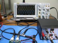
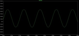
* The first two photos show the Fliege notch filter working just fine with a 5pF capacitor added across the trimpot-to-input resistor. Top trace is the 1KHz input signal, bottom blue trace is the notch filter output. This is a THS4032 board with a 0.047uF / 3.36K + 27R frequency "set" resistor pair, and 33K Q set resistors (Q=5). This board initially oscillated, as shown below, without the 5pF cap.
The 5pF cap (through hole part) across the SMD resistor is the one to the right of the blue trimpot. The resistor soldered on to pin 1 of the THS4032 was an early attempt at solving the oscillation. I lifted that pin on the op amp such that the resistor is in series with the output of that section, in an attempt to try isolating any load capacitance from the op-amp output. It had zero effect of any kind. I tried values from 1R to 1K. The unhooked resistor to the left of the output BNC was another attempt, a 49.9R resistor from output to ground. That did dramatically reduce the amplitude of the oscillation, but didn't eliminate it. I've unhooked it to fully test out this fix.
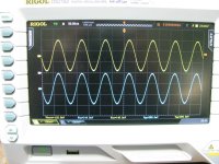
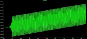
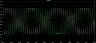
* The next four show the oscillation and board. The 5pF capacitor is removed from R8 and the input BNC to the notch filter is unplugged. For the second and third photos I moved the notch filter output to Ch1 of the scope (yellow) and expanded the time base to get a good look. Notice the amplitude and frequency of the measured oscillation, around 300mVp-p and 25MHz. Both will match up fairly well with the simulated oscillation with 1pF between the leftmost op-amp inputs.
* The final photo is with the 5pF cap soldered back in over R8, with the notch filter input BNC still unhooked and the scope time base expanded to show no oscillation, just random noise.
* The next 3 show the simulation results without the 5pF "stability" capacitor but with 1pF added between the inputs on the leftmost op amp. The oscillation is about 40nS = 25MHz at 500mVp-p, a good matchup with the measured oscillation above. I've run out of photo slots, I'll have to do a part 2 below to show the results with the stability cap.
And a couple of more general observations about the Fliege notch filter. Adding a unity gain buffer at the input would be a good idea, like QuantAsylum did on their twin-T filter. The notch filter would be looking back into nearly 0R output impedance of the buffer. I was also curious if the carbon composition trimpot is responsible for a large portion of the 1mV or so noise in the circuit. It isn't. I tried shorting the sections across, leaving the circuit with just the 0805 thin film resistors. No noticeable change in the noise floor.
My dual-op amp Fliege notch filter board has worked reasonably well with the AD8397 per the posts above. But the THS4032 oscillated in the board, which has been especially curious since the THS4031 worked just fine with no oscillation in the double single V3.0 board.
I've tracked the problem down to what appears to be an extreme sensitivity in the Fliege notch circuit to any coupling capacitance between the inputs on the "leftmost" op amp, the one with a 0.047uF set capacitor in the feedback loop. Like 1pF or 2pF sensitivity - that is all it takes between the inputs to make it an oscillator. The other op amp doesn't show that behavior between the inputs.
A solution I've come up with, which works in actual measurements in the photos below, is 5pF - 10pF of capacitance added across the resistor which goes from the trimpot back to the input of the filter. Works great. Apparently the capacitor restores enough phase margin to stop the ocillations and does not have a measured effect on notch depth. I wanted to post the find in case someone messing with the Fliege notch filter in the future should find this thread looking for an oscillation solution.
Details....
How I found this was kind of funny. I originally didn't realize that AD8397ARDZ had a metal power pad heat sink on the bottom of the chip. When I went to add the proper heat sink foil & vias on a new layout a few days ago I discovered the traces I had underneath the chip.
Yep, I inadvertantly put a metal plate (the power pad) right on top of two traces, with nothing between them but the thin solder mask. Forms a nifty do-it-yourself capacitor. Luckily that power pad is electrically isolated in this particular chip, so nothing would blow up if the solder mask pierced, but it does form a capacitor.So then I was curious what, exactly, a small amount of capacitance between those two particular traces would do and went back to LTSpice. The two traces turned out to be the input of the leftmost op-amp and just 1pF between them was enough to make the filter oscillate. I never had oscillation problems with the actual AD8397ARDZ based board, so the capacitor formed was probably less than 1pF, but the discovery at least showed up a sensitive part of the circuit and a clue as to why the THS4032 / LME49990 / OPA1611 oscillate.
I switched to the AD8397ARZ (no "D"), without the power pad, for that board anyway just to eliminate any potential problem. But for the THS4032 board, which does oscillate, I messed with the sim and bit and found that a small 5pF - 10pF capacitor from the non-inverting input of the leftmost op amp to ground would restore stability. The same capacitor moved instead to the resistor that ties the trimpot back to the input had the same effect. I tried it out with the actual board, below, and the fix works just fine.
Turns out the transfer function for the Fliege notch filter is developed and posted in a couple of nice threads over on allaboutcircuits.com. But that work is modeled with the typical ideal op amp properties. To find this oscillation it will be necessary to add some of the typical op-amp non-ideal parts back to the model, like input resistance, input-output capacitance, output resistance, the input-to-input trace capacitance etc. Lol something that math software will have to chew on awhile to solve the large matrix. It would be nice to be able to extract a pole directly from the math and show that it winds up in the right half plane. In the meantime this experimental fix should do to try it out with the QA400/401.
Photos:
* The first two photos show the Fliege notch filter working just fine with a 5pF capacitor added across the trimpot-to-input resistor. Top trace is the 1KHz input signal, bottom blue trace is the notch filter output. This is a THS4032 board with a 0.047uF / 3.36K + 27R frequency "set" resistor pair, and 33K Q set resistors (Q=5). This board initially oscillated, as shown below, without the 5pF cap.
The 5pF cap (through hole part) across the SMD resistor is the one to the right of the blue trimpot. The resistor soldered on to pin 1 of the THS4032 was an early attempt at solving the oscillation. I lifted that pin on the op amp such that the resistor is in series with the output of that section, in an attempt to try isolating any load capacitance from the op-amp output. It had zero effect of any kind. I tried values from 1R to 1K. The unhooked resistor to the left of the output BNC was another attempt, a 49.9R resistor from output to ground. That did dramatically reduce the amplitude of the oscillation, but didn't eliminate it. I've unhooked it to fully test out this fix.
* The next four show the oscillation and board. The 5pF capacitor is removed from R8 and the input BNC to the notch filter is unplugged. For the second and third photos I moved the notch filter output to Ch1 of the scope (yellow) and expanded the time base to get a good look. Notice the amplitude and frequency of the measured oscillation, around 300mVp-p and 25MHz. Both will match up fairly well with the simulated oscillation with 1pF between the leftmost op-amp inputs.
* The final photo is with the 5pF cap soldered back in over R8, with the notch filter input BNC still unhooked and the scope time base expanded to show no oscillation, just random noise.
* The next 3 show the simulation results without the 5pF "stability" capacitor but with 1pF added between the inputs on the leftmost op amp. The oscillation is about 40nS = 25MHz at 500mVp-p, a good matchup with the measured oscillation above. I've run out of photo slots, I'll have to do a part 2 below to show the results with the stability cap.
And a couple of more general observations about the Fliege notch filter.
Adding a unity gain buffer at the input would be a good idea, like QuantAsylum did on their twin-T filter. The notch filter would be looking back into nearly 0R output impedance of the buffer. I was also curious if the carbon composition trimpot is responsible for a large portion of the 1mV or so noise in the circuit. It isn't. I tried shorting the sections across, leaving the circuit with just the 0805 thin film resistors. No noticeable change in the noise floor.Attachments
-
 IMG_4051.JPG266.8 KB · Views: 77
 -
 IMG_4050.JPG306.7 KB · Views: 74
 -
 IMG_4052.JPG315.5 KB · Views: 80
 -
 IMG_4053.JPG336.5 KB · Views: 69
 -
 IMG_4055.JPG239.4 KB · Views: 76
 -
 IMG_4056.JPG297 KB · Views: 71
 -
 IMG_4060.JPG330.4 KB · Views: 73
 -
 transient plot 1pF between inputs.jpg113.9 KB · Views: 86
 -
 schematic 1pF between inputs osc.jpg185.5 KB · Views: 91
 -
 transient plot 1pF between inputs zoom.jpg41.6 KB · Views: 83
Last edited:
Oscillation solution part 2
I ran out of photo slots in the post above. Here is the Fliege notch filter circuit with the 10pF "stability" capacitor added across the trimpot-to-input resistor. The plot shows no oscillation, just the normal notch filter output. The input signal in this sim is 2KHz while the filter is set up for 1KHz.
In this sim it took 10pF to counteract the 1pF across the input of U4. In the actual circuit measurements above just 4.7pF was enough to do the job and stop the THS4032 from oscillating.
Attachments
OPA1612 has the deepest notch yet! -57dB measured
I've built up one of my dual op-amp Fliege notch filter boards with the OPA1612 chip. It seems to perform better than either the AD8397 or the THS4032. The OPA1612 is the chip QA used in their twin-T notch filter schematic.
When first built up per the TI schematic it oscillated, similar to the THS4032. 11MHz at 600mVp-p. Once again adding 10pF across the trimpot-to-output resistor solved it, same as with the THS4032. In my previous posts I had a typo and called this resistor the trimpot-to-input. It is the trimpot-to-output, R8 on this board. This test working with the OPA1612 here gives me more confidence the fix with work with a range of chips, so I'm going to go ahead and post the Gerbers and BOM for this board this weekend, in case anybody else would like to mess with it.
One other change vs. the previous boards I've posted: the input-to-ground resistor is now 10K rather than the 49.9R that was on the original TI THS4032 evaluation board. It occurred to me that "properly" terminating the 50R coax is pointless at audio frequencies. Everything will be a lumped element, no RF reflections to worry about in the transmission line (coax). So might as well go with an input resistor that doesn't load the signal generator as much. With 10K to ground on the board's input the DC output voltage is still just 3.0mV or so. Recall from past posts that with no input resistor at all (the TI schematic) the output voltage will hit one power rail or the other.
One other interesting thing from experimenting with the board. For fun I tried adding a large 4.99 meg "DC bleed" resistor across the 0.047uF integrator capacitor (ouput to non-inverting input) on the "leftmost" Fliege notch op-amp. I first tried it in LTSpice sim, then tried it on the board with results essentially matching the sim. The resistor kills the notch quality fast. 4.99 meg dropped the notch to about -40dB. So that confirms what TI wrote about the importance of using C0G ceramics for the frequency "set" caps. They said that an X7R dielectric they tried also reduced the notch quality.
Photos:
* The first four photos show the test setup and the oscillation. Input BNC disconnected, just the on-board 10K to ground on the input. Two 9V batteries running at -7.8Vdc and + 8.1Vdc. OPA1612 chip with the circuit right off the T.I. app note. I've gone to the more compact 1/4" square 12 turn pot on this one, a 50R trimmer in this case for a bit more frequency adjust range (vs. 10R in the previous builds). The scope is on 100mV/div so around 11.1MHz at 600mVp-p. This board is built with the 0.047uF / 3.36K + 27R freqency "set" combination for Fo=1KHz, and 34K Q set resistors for a Q of around 5.
* The next two show the 10pF through-hole cap (1% C0G MLCC 50V) soldered across the trimpot-to-output R8 resistor, with the oscillation all gone on the scope. I also took photos with the vertical gain turned way up, time base shrunk and expanded, etc. to show no oscillation anywhere again. I'll omit those this time.
* The final two photos show the notch bottom. The signal generator and input BNC on the board is the top yellow trace again, while the notch filter output is the bottom blue trace. The minimum notch via adjusting the board's frequency trimpot is 1.5mVp-p, best I can make it out through the noise. That first photo is with the blue on 2mV/div while the second photo is at 1mV/div. Keep in mind this scope's vertical amp itself has about 0.75mVp-p of noise, so about half that visible noise is the scope.
The big trick here though is the top (signal input) trace - now 500mV/div. In the previous posts it was all at 200mV/div. The difference is that now with 10K input on the board vs. the previous 49.9R, the signal generator isn't as loaded and I can get a bigger input swing. So while the notch output is about the same as with the previous AD8397 and THS4032 chips at around 2mV, the input producing it is twice as much! Deeper notch. The scope measured the input signal at 1.04Vp-p, so with a 1.5mVp-p minimum notch bottom that would be a -57dB notch, if I've done the math correctly.
I've built up one of my dual op-amp Fliege notch filter boards with the OPA1612 chip. It seems to perform better than either the AD8397 or the THS4032. The OPA1612 is the chip QA used in their twin-T notch filter schematic.
When first built up per the TI schematic it oscillated, similar to the THS4032. 11MHz at 600mVp-p. Once again adding 10pF across the trimpot-to-output resistor solved it, same as with the THS4032. In my previous posts I had a typo and called this resistor the trimpot-to-input. It is the trimpot-to-output, R8 on this board. This test working with the OPA1612 here gives me more confidence the fix with work with a range of chips, so I'm going to go ahead and post the Gerbers and BOM for this board this weekend, in case anybody else would like to mess with it.
One other change vs. the previous boards I've posted: the input-to-ground resistor is now 10K rather than the 49.9R that was on the original TI THS4032 evaluation board. It occurred to me that "properly" terminating the 50R coax is pointless at audio frequencies.
Everything will be a lumped element, no RF reflections to worry about in the transmission line (coax). So might as well go with an input resistor that doesn't load the signal generator as much. With 10K to ground on the board's input the DC output voltage is still just 3.0mV or so. Recall from past posts that with no input resistor at all (the TI schematic) the output voltage will hit one power rail or the other. One other interesting thing from experimenting with the board. For fun I tried adding a large 4.99 meg "DC bleed" resistor across the 0.047uF integrator capacitor (ouput to non-inverting input) on the "leftmost" Fliege notch op-amp. I first tried it in LTSpice sim, then tried it on the board with results essentially matching the sim. The resistor kills the notch quality fast. 4.99 meg dropped the notch to about -40dB. So that confirms what TI wrote about the importance of using C0G ceramics for the frequency "set" caps. They said that an X7R dielectric they tried also reduced the notch quality.
Photos:
* The first four photos show the test setup and the oscillation. Input BNC disconnected, just the on-board 10K to ground on the input. Two 9V batteries running at -7.8Vdc and + 8.1Vdc. OPA1612 chip with the circuit right off the T.I. app note. I've gone to the more compact 1/4" square 12 turn pot on this one, a 50R trimmer in this case for a bit more frequency adjust range (vs. 10R in the previous builds). The scope is on 100mV/div so around 11.1MHz at 600mVp-p. This board is built with the 0.047uF / 3.36K + 27R freqency "set" combination for Fo=1KHz, and 34K Q set resistors for a Q of around 5.
* The next two show the 10pF through-hole cap (1% C0G MLCC 50V) soldered across the trimpot-to-output R8 resistor, with the oscillation all gone on the scope. I also took photos with the vertical gain turned way up, time base shrunk and expanded, etc. to show no oscillation anywhere again. I'll omit those this time.
* The final two photos show the notch bottom. The signal generator and input BNC on the board is the top yellow trace again, while the notch filter output is the bottom blue trace. The minimum notch via adjusting the board's frequency trimpot is 1.5mVp-p, best I can make it out through the noise. That first photo is with the blue on 2mV/div while the second photo is at 1mV/div. Keep in mind this scope's vertical amp itself has about 0.75mVp-p of noise, so about half that visible noise is the scope.
The big trick here though is the top (signal input) trace - now 500mV/div.
In the previous posts it was all at 200mV/div. The difference is that now with 10K input on the board vs. the previous 49.9R, the signal generator isn't as loaded and I can get a bigger input swing. So while the notch output is about the same as with the previous AD8397 and THS4032 chips at around 2mV, the input producing it is twice as much! Deeper notch. The scope measured the input signal at 1.04Vp-p, so with a 1.5mVp-p minimum notch bottom that would be a -57dB notch, if I've done the math correctly.Attachments
Last edited:
skidave - I agree, time to find out how clean the passband is, for all three chips (THS4032 / AD8397 / OPA1612). I'm also curious what the QA will show for noise floor with the notch in the circuit. I think I'm going to test some different power supply levels with the Fliege notch too, since the OPA1612 is specified all the way up to +/-18Vdc rails.
I'm also curious what the QA will show for noise floor with the notch in the circuit. I think I'm going to test some different power supply levels with the Fliege notch too, since the OPA1612 is specified all the way up to +/-18Vdc rails.V1.0 Gerbers and BOM, V2.0 likely
Here are the Gerbers & BOM for the V1.0 Fliege notch filter dual-op amp board in the posts above. The BOM has three different sets of capacitors and resistors that all make a 1.0KHz notch. One set is based on a 0.047 (1% C0G 0805) capacitor, another on a 0.022uF, and the third on a 0.01uF. These are the three 1% C0G 0805 in stock at Mouser right now that are 10nF or above. They do also have a 0.1uF 1% C0G but that is a 1206 size and goes for $6.50.
But... if anyone is thinking of having a board made you might want to wait. Below is a V2.0 I'm working on and will probably send out for fabrication one of these days to test. Teh filter is done but the power supply is still a work in progress. If this one works I'll post the Gerbers for it too. Some of the new stuff:
* A stack of 6 parallel frequency "set" 0.047uf 1% C0G capacitors to further improve the tolerance (and further reduce ESR and reduce the tempco variation of any one element). A cool math trick. Turns out that when resistors or capacitors are placed in series or parallel the tolerance improves. In this case the 1% drops to around 0.4%. This fellow has worked out a statistical derivation of the formula. The result turns out to be the original tolerance divided by the square root of the number of parallel (or series) elements:
Combining Multiple Resistors to Improve Tolerance
His derivation is for resistors, but it would apply equally well to capacitors.
* Related to the above, increasing the value of the frequency "set" capacitors results in a much smaller frequency "set" resistorvalue, around 560R in this case for the stack of 6 0.047uF frequency "set" capacitors. Having resistors less than 1K in series with the input of the op amps helps reduce any input impedance distortion effects. Here is a paper on it from Linear Technology:
http://www.linear.com/docs/4280
As an added bonus the Johnson noise is reduced by the smaller resistor values.
* Fits in a metal B2-080 Box Enclosures case to (finally) properly shield the thing. Also turns out that 80mmx100mm here is still just $49 for 5 boards (and maybe 10, haven't checked) at pcbway.com.
* An input buffer op-amp is added to provide 0R for the filter circuit parts lookinig back into the input.
* Has a place for an alternate long and flat type trimpot with the screw at the end, placed between the BNC connectos. This allows the frequency to be adjusted via a hole in the front panel even after the board is boxed up in the case. Turns out Bourns has a "front panel mount nose piece" for these trimmers which even adds threads for a front panel nut.
* Placeholders for several "test" parts to allow messing around with the board. There are places for (the 10pF) 0805 caps across both trimpot feed resistors, places for series resistors on the op-amp output, etc. Placeholder for a bleeder resistor across the integration capacitor.
* Still includes two battery snaps (and the four corner mounting holes) for tabletop use, but now they are end-mount snaps soldered right on the board to eliminate any connection wires to the battery snaps. Batteries won't fit in the case though, so...
* Internal power supply. LDO regs heat sinked to the rear panel. Adjsutable regulators can go all the way up to +/-18Vdc. Alternately the power jack can be left off and power wires from and external supply run through the same rear panel hole.
If anyone out there reading this wants to have some DIY fun with the Fliege notch filter, here is a suggestion for a high-tech V3.0: use a bandpass filter and a phase locked loop chip to track the actual frequency of the fundamental, including tracking any small amount of drift in the signal generator over time. Then use that to automatically adjust the frequency of the Fliege notch to track the fundamental. There is an EDN paper out on Google with something similar - which apparently works - using a universal switched capacitor filter for the notch. Unfortunately a switched cap filter would likely not have a low enough THD in the passband for this application.
Here are the Gerbers & BOM for the V1.0 Fliege notch filter dual-op amp board in the posts above. The BOM has three different sets of capacitors and resistors that all make a 1.0KHz notch. One set is based on a 0.047 (1% C0G 0805) capacitor, another on a 0.022uF, and the third on a 0.01uF. These are the three 1% C0G 0805 in stock at Mouser right now that are 10nF or above. They do also have a 0.1uF 1% C0G but that is a 1206 size and goes for $6.50.
But... if anyone is thinking of having a board made you might want to wait.
Below is a V2.0 I'm working on and will probably send out for fabrication one of these days to test. Teh filter is done but the power supply is still a work in progress. If this one works I'll post the Gerbers for it too. Some of the new stuff:* A stack of 6 parallel frequency "set" 0.047uf 1% C0G capacitors to further improve the tolerance (and further reduce ESR and reduce the tempco variation of any one element). A cool math trick.
Turns out that when resistors or capacitors are placed in series or parallel the tolerance improves. In this case the 1% drops to around 0.4%. This fellow has worked out a statistical derivation of the formula. The result turns out to be the original tolerance divided by the square root of the number of parallel (or series) elements:Combining Multiple Resistors to Improve Tolerance
His derivation is for resistors, but it would apply equally well to capacitors.
* Related to the above, increasing the value of the frequency "set" capacitors results in a much smaller frequency "set" resistorvalue, around 560R in this case for the stack of 6 0.047uF frequency "set" capacitors. Having resistors less than 1K in series with the input of the op amps helps reduce any input impedance distortion effects. Here is a paper on it from Linear Technology:
http://www.linear.com/docs/4280
As an added bonus the Johnson noise is reduced by the smaller resistor values.
* Fits in a metal B2-080 Box Enclosures case to (finally) properly shield the thing.
Also turns out that 80mmx100mm here is still just $49 for 5 boards (and maybe 10, haven't checked) at pcbway.com. * An input buffer op-amp is added to provide 0R for the filter circuit parts lookinig back into the input.
* Has a place for an alternate long and flat type trimpot with the screw at the end, placed between the BNC connectos. This allows the frequency to be adjusted via a hole in the front panel even after the board is boxed up in the case. Turns out Bourns has a "front panel mount nose piece" for these trimmers which even adds threads for a front panel nut.
* Placeholders for several "test" parts to allow messing around with the board. There are places for (the 10pF) 0805 caps across both trimpot feed resistors, places for series resistors on the op-amp output, etc. Placeholder for a bleeder resistor across the integration capacitor.
* Still includes two battery snaps (and the four corner mounting holes) for tabletop use, but now they are end-mount snaps soldered right on the board to eliminate any connection wires to the battery snaps. Batteries won't fit in the case though, so...
* Internal power supply. LDO regs heat sinked to the rear panel. Adjsutable regulators can go all the way up to +/-18Vdc. Alternately the power jack can be left off and power wires from and external supply run through the same rear panel hole.
If anyone out there reading this wants to have some DIY fun with the Fliege notch filter, here is a suggestion for a high-tech V3.0: use a bandpass filter and a phase locked loop chip to track the actual frequency of the fundamental, including tracking any small amount of drift in the signal generator over time. Then use that to automatically adjust the frequency of the Fliege notch to track the fundamental. There is an EDN paper out on Google with something similar - which apparently works - using a universal switched capacitor filter for the notch. Unfortunately a switched cap filter would likely not have a low enough THD in the passband for this application.
Attachments
Last edited:
adgr, how about some loop back results using your QA and the frequency response portion. Also, maybe a DUT with notch and w/out notch using the FFT.
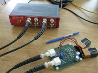
I finally have all the pieces together to do this test from back in February.
This is with the new QA401 auido analyzer I picked up a few weeks ago and a Fliege notch V3.0 board with an AD8397 chip. I have a new V4.0 board that just arrived from the fab but haven't had a chance to build one up yet.Photos - keep in mind you can click on the lower left corner to zoom these up:
* The photo is the test setup. The QA401 is being run single-ended with the unused input shorted with a BNC shorting cap.
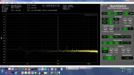
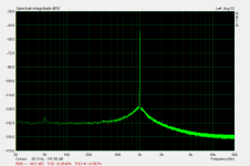
* The first screen grab is the QA401 in loopback, for reference. This is with the generator set for -10dBV. The usual QA401 2nd, 3rd, and 4th harmonics appear.
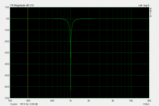
* Next is the deepest Fliege notch point with the current frquency setting, 998.8Hz at -70dBV. Rounding in the QA401 generator is turned off here to get an exact frequency. Since the input is -10dBV that is a -60dBV notch. However keep in mind the Fliege notch frequency is adjustable with the trimpot. With some adjusting I could get it even closer to 1.00KHz. As for how I found this point, see the QA401 frequency response plot below. The frquency shows up at the top of the QA401 screen.
* Next is the same at 1Hz higher, 999.8Hz. The notch depth lessens to -55dBV, which shows the notch well is fairly sharp! Just 1Hz away from the notch bottom the notch well is 15dBV higher.
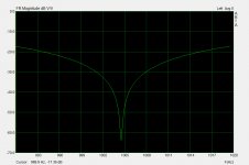
* Next is a QA401 frequency response plot around the notch, going from 950Hz to 1050KHz in 2Hz steps. From the plot the middle of the notch appears to be between 998 and 1000Hz.
For all the details on how to do these QA401 FR plots, see my post #11 in the Akerman-Mossberg differential notch filter thread:
http://www.diyaudio.com/forums/equi...erential-notch-q401-part-1-a.html#post4709636
Just as with that posting, I'm using QA's suggestion of turning off generator rounding to get an exact frquency and using the flat-top window for frequency accuracy.
* So next is running the same FR plot but shrunk down to 990Hz to 1010Hz to better characterize the notch mid-point. The 998.8Hz line clearly shows as the middle, which is why I started with that plot here, above. But keep in mind the Fliege is frequency adjustable - this is just where the trimpot is set at the moment.
Well.... in summary it looks pretty good except for that 2nd harmonic! With the 1KHz fundamental -60dB down I would expect those 2nd and 3rd harmonics in the QA401 not to show up anymore. That is kind of the purpose of using the notch filter. Since a 2nd is showing up I have to conclude that is coming from the Fliege filter and not the QA401, likely the AD8397 chip. I've have to try this test again with some other chips in the board. But the 3rd hamonic is gone and the higher ones are significantly diminished.
Attachments
-
 IMG_4165.JPG282 KB · Views: 302
 -
 loopback 1KHz -10dBV with rnd.jpg239.1 KB · Views: 283
 -
 Fliege AD8397 998.8 Hz -10dBV input no rnd.jpg279.6 KB · Views: 279
 -
 Fliege AD8397 999.8 Hz -10dBV input no rnd.jpg236.4 KB · Views: 273
 -
 Fliege AD8397 QA401 FR 950Hz 1050Hz 2Hz no rnd flat top.jpg218.6 KB · Views: 279
 -
 Fliege AD8397 QA401 FR 990Hz 1010Hz 0.2Hz no rnd flat top.jpg265.7 KB · Views: 121
Last edited:
Just wondering if you got better results with other opamps.
I have a QA401 and want to improve the level I can measure through notch filter also. So I'm thinking between passive twin-t, active twin-t, and the Fliege.
Would be interested in your comments among them, given your experience on the topic.
Thanks and regards.
I have a QA401 and want to improve the level I can measure through notch filter also. So I'm thinking between passive twin-t, active twin-t, and the Fliege.
Would be interested in your comments among them, given your experience on the topic.
Thanks and regards.
Just wondering if you got better results with other opamps.
To be honest I managed to get side-tracked with a couple of other projects (Super CMOY in the headphone forum) and haven't done much more with the notch filters.
I think the most promising one of the bunch is the Akerberg Mossberg fully differential notch filter board I built:
http://www.diyaudio.com/forums/equi...g-fully-differential-notch-q401-part-1-a.html
It worked with batteries, but but I have it designed to use either batteries or the on-board voltage regulator with an external DC feed. I have it set up so the "noisy" stuff for the power supply is in the separate metal box, then cables the unregulated +/-15Vdc + ground over via an RJ45 connector on each box. I wanted to do further testing with the external power feed, but the separate power supply board took 3 more board turns to finally get it right.
Turns out there are two different RJ45 pin-outs depending on if it follows CAT5 or not. Who knew, lol.As for the Fliege, TI is discontinuing those LME49990s that oscillated. The AD chip was about the best performer.
I haven't tried a passive twin-T, but I think I did design and fabricate an active one. I don't believe I ever tested it though, so unfortunately no results to share there.
Last edited:
I made one for experimentation, using 2 layer PCB (4 layer too expensive) and OPA1612. Seems to work ok, no oscillation
Attachments
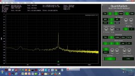
Attached is the spectrum of a 1KHz Viktor Oscillator (@0.5Vrms out) with and without the Fliege notch.
There is already a 26dB post-notch gain stage, but it's still not enough and all the harmonics are hidden within the noise floor, so I can't estimate the THD. I probably need a 40dB or even 60dB gain stage.
There is already a 26dB post-notch gain stage, but it's still not enough and all the harmonics are hidden within the noise floor, so I can't estimate the THD. I probably need a 40dB or even 60dB gain stage.
Attachments
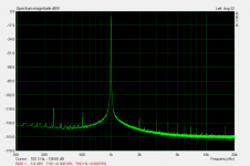
Attached is the spectrum of a 1KHz Viktor Oscillator (@0.5Vrms out) with and without the Fliege notch.
Hey **big** congratulations on your Fliege!
Better than I've been able to do so far. Maybe the 1612 is the key to getting rid of the oscillations. I'll have to go back and see if I ever tried the 1612. Maybe the two layer is helping too. I had two power planes and the ground plane. I was wondeirng if I had signal coupling to those planes and tried notch-outs all over the place.I see you included the frequency adjust trimmer too! That seemed to be the most sensitive part (regarding oscillations) on my boards. And it looks like you used an AD8429 for the gain stage - I don't think I've heard of that chip before! Looks pretty good from a quick read of the data sheet.
Last edited:
> I probably need a 40dB or even 60dB gain stage.
If the noise came from your filter and not your gain stage, increasing the gain will not solve your problem.
The only solution is to reduce noise and distortion of your active filter.
Also assume that the Viktor oscillator is << -140dB, your first meaurement is showing the distortion of your analyser.
So that will also mask any results < -130dB.
Not much you can do .....
Patrick
ThanksHey **big** congratulations on your Fliege!
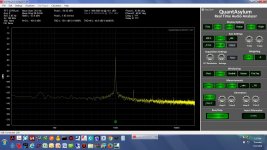
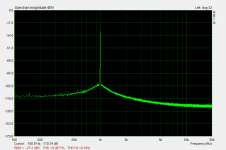
With a notch attenuation of 52dB and a post-notch amp of 38dB (80x), I got the attached. A little math says that it has measured down to -138dB THD.
Still not capable to measure the Viktors, but already better than expected. Grounded shielding of all parts involved is mandatory, otherwise the results deteriorate substantially.
Attachments
Last edited:
Something funny - I just went back to refresh my memory on where I stood with the Fliege stuff. Turns out I never did build up the V4.0 boards that I got back in May, back in post #71! Looks like I did try an OPA1612 with the V3.0 board and it worked, *if* I added the extra 10pF capacitor by the trimpot. So definite congratulations on getting yours stable right from the first try!
I'll have to build up one of these V4.0s with a 1612 and see what happens, I'm curious now. These are designed to fit a Box Enclosures B2-080 aluminum case, with external power feed from the rear RJ45, or stand-along with the on-board 9V battery snaps. The batteries can be fed directly through the chips, or via the two voltage regulators. The external RJ45 feed has to go through the vregs. The board is 4 layer with the two power planes and ground plane, and I didn't notch anything out on this one, so I'll probably get capacitive coupling between the traces and those planes. Looks like I ordered the layers such that the second layer down, under the parts, is ground. Then 3rd and 4th (bottom foil) are the power planes. At least the OPA1612 is 40MHz GBW and not the 110 for the LME49990. That alone should help with oscillations. Intesting thing though, I think that TI paper made the statement that 100MHz + GBW was needed for a Fliege up to 20KHz. I'll have to go back and review that. Your results prove that isn't true!
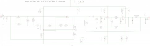
The long rows of chip caps are to to build up the frequency set capacitors with many in parallel. Cheaper than one big one with C0G, and decreases the tolerance if stacked in parallel. Lol, probably adds a boatload of inductance through.
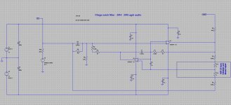
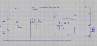
On here IC1 is an input (unity gain) buffer, so the Fliege could look back into zero ohms. That (sensitivity to) input impedance issue seemed to keep coming up with the Fliege, so I decided to solve it once and for all. IC2 is the (dual) Fliege chip, IC5 is the optional output gain stage, and IC6 is a BUF634 that IC5 can optionally be looped around, just to drive more output cable capacitance. IC3 and IC4 are the voltage regulators heat sinked to the rear panel. The "chips tested to work" text in the middle that has the OPA1612 listed is a carry-over from V3.0. V4.0 here started with the V3.0 layout.
I'll have to build up one of these V4.0s with a 1612 and see what happens, I'm curious now.
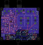
These are designed to fit a Box Enclosures B2-080 aluminum case, with external power feed from the rear RJ45, or stand-along with the on-board 9V battery snaps. The batteries can be fed directly through the chips, or via the two voltage regulators. The external RJ45 feed has to go through the vregs. The board is 4 layer with the two power planes and ground plane, and I didn't notch anything out on this one, so I'll probably get capacitive coupling between the traces and those planes. Looks like I ordered the layers such that the second layer down, under the parts, is ground. Then 3rd and 4th (bottom foil) are the power planes. At least the OPA1612 is 40MHz GBW and not the 110 for the LME49990. That alone should help with oscillations. Intesting thing though, I think that TI paper made the statement that 100MHz + GBW was needed for a Fliege up to 20KHz. I'll have to go back and review that. Your results prove that isn't true! The long rows of chip caps are to to build up the frequency set capacitors with many in parallel. Cheaper than one big one with C0G, and decreases the tolerance if stacked in parallel. Lol, probably adds a boatload of inductance through.
On here IC1 is an input (unity gain) buffer, so the Fliege could look back into zero ohms. That (sensitivity to) input impedance issue seemed to keep coming up with the Fliege, so I decided to solve it once and for all. IC2 is the (dual) Fliege chip, IC5 is the optional output gain stage, and IC6 is a BUF634 that IC5 can optionally be looped around, just to drive more output cable capacitance. IC3 and IC4 are the voltage regulators heat sinked to the rear panel. The "chips tested to work" text in the middle that has the OPA1612 listed is a carry-over from V3.0. V4.0 here started with the V3.0 layout.
Attachments
Last edited:
- Home
- Design & Build
- Equipment & Tools
- Fliege 1kHz notch filter project PCB