10R trimmer, 5x and 20x post-filter gain
marce - I value your layout suggestions! Thank you for all the good tips. You clearly have lots and lots of experience with what works and what doesn't with layout.
Well... I may give those separate voltage regulators more thought then! I did some work on the dual channel version today, removing all the cutouts, and shrinking loop sizes down. It does look like there may be adequate room at the base for voltage regulators on each. That should help eliminate any crosstalk. Both notch filters would be looking back into the output impedance other their own vregs.
Speaking of datasheets suggesting notching, I was reading through the AD8397 data sheet today
http://www.analog.com/media/en/technical-documentation/data-sheets/AD8397.pdf (opens PDF)
and I actually ran into another one page 11 under "Layout Considerations":
"Removing the ground plane from all layers in the immediate area of the amplifier helps to reduce stray capacitances"
I'm going with your suggestion on this one though. I've removed the notches. Just one solid ground plane now.")
marce - I value your layout suggestions! Thank you for all the good tips. You clearly have lots and lots of experience with what works and what doesn't with layout.
Well... I may give those separate voltage regulators more thought then! I did some work on the dual channel version today, removing all the cutouts, and shrinking loop sizes down. It does look like there may be adequate room at the base for voltage regulators on each. That should help eliminate any crosstalk. Both notch filters would be looking back into the output impedance other their own vregs.
Speaking of datasheets suggesting notching, I was reading through the AD8397 data sheet today
http://www.analog.com/media/en/technical-documentation/data-sheets/AD8397.pdf (opens PDF)
and I actually ran into another one page 11 under "Layout Considerations":
"Removing the ground plane from all layers in the immediate area of the amplifier helps to reduce stray capacitances"
I'm going with your suggestion on this one though. I've removed the notches. Just one solid ground plane now.
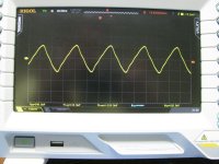
10R trimmer, 5x and 20x post-amp, -54dB notch part 1
I had some time today to mess with the V3.0 board with the two single op-amps a bit more, still with the THS4031's in place.
I swapped out the 50R trimmer for a 10R trimmer to give more fine-adjust rangle. Works great. I now am able to go about a full turn in each direction back and forth at the bottom of the notch (25 turn trimmer) to fine-tune the notch.
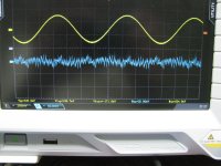
I've hooked in the post-filter-amplifier to boost the notch filter output and help find the exact notch depth through the scope noise (and EMI, the board is still not in a shielded box). That also worked great. From the photos below, with a 20x voltage gain after the notch filter, it now appears the notch is actually -54dB real-world, vs. the sim of -73dB. If the AD8397 adds to that (sims at -92dB) that may be somewhere around -70dB!
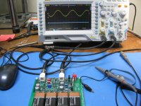
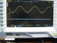
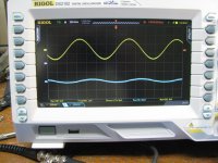
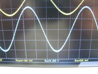
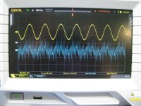
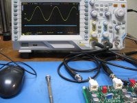
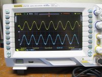
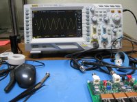
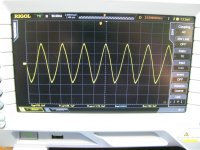
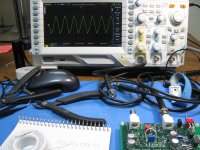
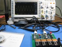
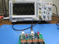
* The first two photos 3932 & 3933 are the test setup. The signal generator is the top yellow trace again while the notch filter through the post-filter-amp is the bottom blue trace. Turns out the generator can do 1/10Hz and 1/100 Hz increments. The trace in this photo is with 1.00000KHz and 200mV/div on both scope traces.
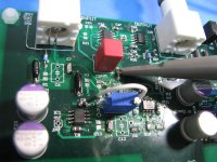
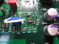
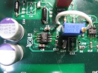
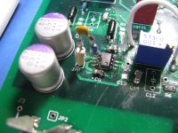
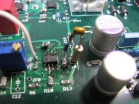
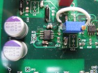
* The next photo 3935 shows what I did to hook in the post-filter-amplifier. The 49.9R resistor R18 that was in series with the filter output to the out BNC connector is moved to previously-blank R28 position, which is the output of the amplifier. This breaks the direct link from the notch filter output to the output BNC (R18) and connects the amplifier output instead to the output BNC (R28). This is why I used through-hole for these two resistors, just makes it easy to get them out with the vacuum desolderer.
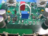
On the input side the jumper J7 and blocking capacitor C21 are installed to forward the notch filter output to the amplifier input. Jumper J7 also makes a handy place to hook a scope probe, as shown below, when verifying amplifier gain. The OPA140 + BUF634 non-inverting amp has 2.49K and 499R gain set resistors (2.49K is the feedback resistor), so 2490/499 = 5x voltage gain to start. Later in the photos below I swap out the 2.49K R25 for a 10K to give 20x voltage gain. With C21 in now the resulting output has just the 30 microvolts or so from the OPA140 + BUF634 combination. Completely eliminates the mV level offset from the notch filter's THS4031 chips.
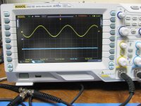
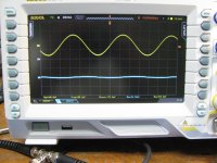
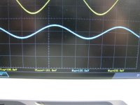
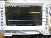
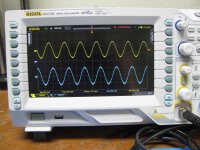
* 3936 and 3937 are 1.00010KHz and 0.9999KHz. This answers the good question that came up previously about what happens with 1/10Hz variation, rather than the 1Hz minimum I did previously. I also tried 1/100Hz variation, but it was just too small to record any useful visual change in the notch. The 1/10Hz here is visible though. Kind of hard to tell in the photo, but in varying the generator frequency back and forth from 1.00010KHz to 1.00000KHz the slight sine wave is definitely there. Glad that suggestion came up! So moving +/- 1/10Hz off from the notch center frequency does start moving you out of the notch well bottom, but +/-1/100Hz doesn't to any (visible) significant degree.
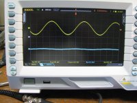
* 3938 & 3939 are 1.00030KHz and 0.99970 (+/- 3/10Hz).
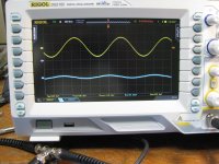
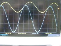
* 3940 * 3941 are 1.00100KHz and 0.9990KHZ (+/- 1HZ). Now this is the same frequency variation I posted photos of previously in post #10 above, the 4th and 5th photo. BUT... here the notch output is going through the 5x voltage gain amplifier. The scope in these two photos (blue trace) and the one previously are on 200mV/div. Compare the two pairs of photos and the 5x voltage gain shows right up.
I had some time today to mess with the V3.0 board with the two single op-amps a bit more, still with the THS4031's in place.
I swapped out the 50R trimmer for a 10R trimmer to give more fine-adjust rangle. Works great. I now am able to go about a full turn in each direction back and forth at the bottom of the notch (25 turn trimmer) to fine-tune the notch.
I've hooked in the post-filter-amplifier to boost the notch filter output and help find the exact notch depth through the scope noise (and EMI, the board is still not in a shielded box). That also worked great. From the photos below, with a 20x voltage gain after the notch filter, it now appears the notch is actually -54dB real-world, vs. the sim of -73dB. If the AD8397 adds to that (sims at -92dB) that may be somewhere around -70dB!
* The first two photos 3932 & 3933 are the test setup. The signal generator is the top yellow trace again while the notch filter through the post-filter-amp is the bottom blue trace. Turns out the generator can do 1/10Hz and 1/100 Hz increments. The trace in this photo is with 1.00000KHz and 200mV/div on both scope traces.
* The next photo 3935 shows what I did to hook in the post-filter-amplifier. The 49.9R resistor R18 that was in series with the filter output to the out BNC connector is moved to previously-blank R28 position, which is the output of the amplifier. This breaks the direct link from the notch filter output to the output BNC (R18) and connects the amplifier output instead to the output BNC (R28). This is why I used through-hole for these two resistors, just makes it easy to get them out with the vacuum desolderer.
On the input side the jumper J7 and blocking capacitor C21 are installed to forward the notch filter output to the amplifier input. Jumper J7 also makes a handy place to hook a scope probe, as shown below, when verifying amplifier gain.
The OPA140 + BUF634 non-inverting amp has 2.49K and 499R gain set resistors (2.49K is the feedback resistor), so 2490/499 = 5x voltage gain to start. Later in the photos below I swap out the 2.49K R25 for a 10K to give 20x voltage gain. With C21 in now the resulting output has just the 30 microvolts or so from the OPA140 + BUF634 combination. Completely eliminates the mV level offset from the notch filter's THS4031 chips.* 3936 and 3937 are 1.00010KHz and 0.9999KHz. This answers the good question that came up previously about what happens with 1/10Hz variation, rather than the 1Hz minimum I did previously. I also tried 1/100Hz variation, but it was just too small to record any useful visual change in the notch. The 1/10Hz here is visible though. Kind of hard to tell in the photo, but in varying the generator frequency back and forth from 1.00010KHz to 1.00000KHz the slight sine wave is definitely there. Glad that suggestion came up! So moving +/- 1/10Hz off from the notch center frequency does start moving you out of the notch well bottom, but +/-1/100Hz doesn't to any (visible) significant degree.
* 3938 & 3939 are 1.00030KHz and 0.99970 (+/- 3/10Hz).
* 3940 * 3941 are 1.00100KHz and 0.9990KHZ (+/- 1HZ). Now this is the same frequency variation I posted photos of previously in post #10 above, the 4th and 5th photo. BUT... here the notch output is going through the 5x voltage gain amplifier. The scope in these two photos (blue trace) and the one previously are on 200mV/div. Compare the two pairs of photos and the 5x voltage gain shows right up.
Attachments
-
 IMG_3932.JPG657 KB · Views: 207
 -
 IMG_3933.JPG565.6 KB · Views: 198
 -
 IMG_3935_1.jpg612.9 KB · Views: 198
 -
 IMG_3936.JPG502.3 KB · Views: 199
 -
 IMG_3937.JPG513.2 KB · Views: 190
 -
 IMG_3939.JPG537.3 KB · Views: 49
 -
 IMG_3938.JPG508.9 KB · Views: 51
 -
 IMG_3940.JPG549.3 KB · Views: 53
 -
 IMG_3941.JPG537.7 KB · Views: 60
Last edited:
part 2, 18.3x gain -52dB notch
I ran out of photo slots in the post above. Part 2. Above I assumed 20x voltage gain for a -54dB notch. Here it measures to be 18.3x, which calculates to a notch depth of -52dB.
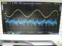
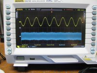
* The first three photos show a measured confirmation of the voltage gain of the OPA140 + BUF634 post-notch-filter amplifier. The first photo is the output of the amp (blue trace), what is on the board's output BNC jack going to the scope. In blue, below the blue trace, you can see the scope has measured a peak of around 592mV. It actually bounced back and forth between 600mV and 592mV, so I'm going to use 600mV here to make things easy. I've changed the signal generator for these photos to 1.02000KHz to allow a sine wave to show up for the voltage gain measurements.
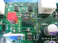
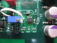
In the second photo I'm measuring the input to the amplifier, which is the output of the Fliege notch filter, at the point on the PCB shown in the 3rd photo. Here I've just replaced the second scope input with a probe and latched it onto J7. The scope now calculates 120mV peak. Doing the math gives 600mV/120mV =5x voltage gain, as expected. At at this point I've just realized I said the wrong thing in the previous post, the feedback resistor I built it with here is 2K rather than 2.49K. (1 + 2K/499R) = 5x for the non-inverting stage. 2.49K is R27 the minimum load resistor (to ground) on the output that I like to have on these op-amp plus buffer loops.
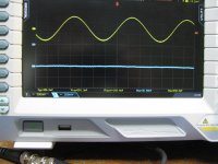
* 5x voltage gain turned out to still be insufficient to see the bottom of the notch well while vaying the generator frequency back and forth +/- 1Hz (and +/= 0.1Hz now). So I bumped it up to 18.3x in the next photo. 2.2V / 120mv = 18.3x .
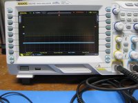
* In the final two photos I've set the signal generator back to the 1.00000KHz notch frequency, now with the 18.3x voltage gain applied tothe Fliege notch filter output. The first photo is with 50mV/division on the scope while the second is with 20mV/div. It is hard to tell from that 20mV/div photo, but by varying the frequency trimmer back and forth the minimum notch bottom output I can obtain appears to be around 10mV peak, with the 18.3x voltage gain applied. With the 220mV peak input signal from the generator (still the yellow trace on the scope) that should give somewhere around (10mV/18.3)/220mV = 0.002484 which is -52dB.
LOL - if anyone happened to see that I just deleted and re-posted this post, here is what happened. On the first try I got my input signals mixed up in the math and thought the circuit was rather unexpectedly producing a -72dB notch, which would match the sim, but which I never would expect to happen in a real-world circuit. Well it just so happens that the peak from the signal generator going into the Fliege notch filter (220mV, yellow trace) and the test output signal from the amplifier I had produced above by de-tuning to 1020KHz (2200mV, blue trace) were off my one decimal place and I got them mixed up. Do the math with a 2200mV input signal and you get an (erroneous) -72dB notch.
I ran out of photo slots in the post above.
Part 2. Above I assumed 20x voltage gain for a -54dB notch. Here it measures to be 18.3x, which calculates to a notch depth of -52dB.* The first three photos show a measured confirmation of the voltage gain of the OPA140 + BUF634 post-notch-filter amplifier. The first photo is the output of the amp (blue trace), what is on the board's output BNC jack going to the scope. In blue, below the blue trace, you can see the scope has measured a peak of around 592mV. It actually bounced back and forth between 600mV and 592mV, so I'm going to use 600mV here to make things easy. I've changed the signal generator for these photos to 1.02000KHz to allow a sine wave to show up for the voltage gain measurements.
In the second photo I'm measuring the input to the amplifier, which is the output of the Fliege notch filter, at the point on the PCB shown in the 3rd photo. Here I've just replaced the second scope input with a probe and latched it onto J7. The scope now calculates 120mV peak. Doing the math gives 600mV/120mV =5x voltage gain, as expected. At at this point I've just realized I said the wrong thing in the previous post, the feedback resistor I built it with here is 2K rather than 2.49K. (1 + 2K/499R) = 5x for the non-inverting stage. 2.49K is R27 the minimum load resistor (to ground) on the output that I like to have on these op-amp plus buffer loops.
* 5x voltage gain turned out to still be insufficient to see the bottom of the notch well while vaying the generator frequency back and forth +/- 1Hz (and +/= 0.1Hz now). So I bumped it up to 18.3x in the next photo. 2.2V / 120mv = 18.3x .
* In the final two photos I've set the signal generator back to the 1.00000KHz notch frequency, now with the 18.3x voltage gain applied tothe Fliege notch filter output. The first photo is with 50mV/division on the scope while the second is with 20mV/div. It is hard to tell from that 20mV/div photo, but by varying the frequency trimmer back and forth the minimum notch bottom output I can obtain appears to be around 10mV peak, with the 18.3x voltage gain applied. With the 220mV peak input signal from the generator (still the yellow trace on the scope) that should give somewhere around (10mV/18.3)/220mV = 0.002484 which is -52dB.
LOL - if anyone happened to see that I just deleted and re-posted this post, here is what happened. On the first try I got my input signals mixed up in the math and thought the circuit was rather unexpectedly producing a -72dB notch, which would match the sim, but which I never would expect to happen in a real-world circuit. Well it just so happens that the peak from the signal generator going into the Fliege notch filter (220mV, yellow trace) and the test output signal from the amplifier I had produced above by de-tuning to 1020KHz (2200mV, blue trace) were off my one decimal place and I got them mixed up. Do the math with a 2200mV input signal and you get an (erroneous) -72dB notch.
Attachments
Last edited:
marce - I value your layout suggestions!...
---
Speaking of datasheets suggesting notching, I was reading through the AD8397 data sheet today
http://www.analog.com/media/en/technical-documentation/data-sheets/AD8397.pdf (opens PDF)
and I actually ran into another one page 11 under "Layout Considerations":
"Removing the ground plane from all layers in the immediate area of the amplifier helps to reduce stray capacitances"
I'm going with your suggestion on this one though. I've removed the notches. Just one solid ground plane now.
Just a reflection - if a layout suggestion from the chip designer for some reason wouldn't matter for the layout at hand wouldn't it be better to incorporate it as not doing it might lock one harder to the exact circuit? A change might call for the suggestion to be in place.
Regards
As with all high speed applications, pay careful attention to printed circuit board (PCB) layout to prevent associated board parasitics from becoming problematic. The PCB should have a low impedance return path (or ground) to the supply. Removing the ground plane from all layers in the immediate area of the amplifier helps to reduce stray capacitances. The signal routing should be short and direct in order to minimize the parasitic inductance and capacitance associated with these traces. Locate termination resistors and loads as close as possible to their respective inputs and outputs. Keep input traces as far apart as possible from the output traces to minimize coupling (crosstalk) though the board.
As with all high speed applications, pay careful attention to printed circuit board (PCB) layout to prevent associated board parasitics from becoming problematic.
I have quoted the relevant line twice, as I stated in my earlier post high speed is a different kettle of fish to what you are doing with slow audio signals. If you were doing high speed then the rules do change slightly, but you are not so don't worry about high speed design rules...
This is low level analogue so no need to remove the ground area. I've done layout now for 30+ years and do the analogue layout for some interesting projects and as I stated earlier, the only time I have made holes in the ground plane is around input pins when doing very high speed analogue (over a million times faster than audio). So when reviewing data sheets look at the whole reference, both digital and analogue layout will vary depending on signal speeds, audio is low speed (very).
It is quite easy to determine how bad the effect can be using my previous reference where the copper in removed from under the input pin (almost microwave design, it was a test board for testing the new sensors for space exploration). Pin with ground plane creates a 0.1pF capacitor (approx.) at 20K top end of audio the Xc = 80Mohms at 20MHz the reactance is 80KOhms and at 200MHz it is only 8KOhms, so as frequency increases the Xc decreases and coupling becomes more of an issue as do ALL parasitics including inductance and capacitance, you may also get problems with skin effect at these higher frequencies, but you aren't doing high speed analogue design so don't worry.....
Some more revelent (irrevelant) further reading
http://www.x2y.com/filters/TechDay0...log_Designs_Demand_GoodPCBLayouts _JohnWu.pdf
Technical Articles/Talks
Analog Devices: Analog Dialogue: Ask The Applications Engineer - 12
http://www.calex.com/pdf/4ground_shield.pdf
http://qtwork.tudelft.nl/~schouten/linkload/grounding.pdf
http://www.celectronics.com/pdf/IEEE11-9-05.pdf
http://www.analog.com/media/en/tech...14948960492698455131755584673020828AN_345.pdf
This again is more for high speed design, but a good reference.
http://www.analog.com/library/analogDialogue/archives/39-09/layout.pdf
Decreasing parasitic capacitance in IC layouts | EDN
LearnEMC - Electric Field Coupling
http://personal.maths.surrey.ac.uk/st/J.Deane/pdf/capcalc.pdf
http://ecee.colorado.edu/~mcleod/teaching/EandM3400/Lab Book/Lab_5.pdf
http://www.leonardo-energy.org/sites/leonardo-energy/files/root/EPQU/JVol12No1/kovacova.pdf
When you get to high speed analogue you are getting into the realms of RF layout!!!! Here all sanity leaves the room
LME49990 swapped back in, plus datasheet output comp network
Hey guys, thanks for the comments! I'll read through tomorrow (midnight here now).
So now that V3.0 works well with the THS4031 chips I couldn't resist swapping the LME49990 back in, one at a time, to see what happens. I also wanted to try out that LRC output compensation network the LME49990 datasheet shows.
The results: swapping out IC4 in the schematic (the rightmost Fliege notch op-amp, the one driving the trimmer pot) from THS4031 to LME49990, it (still) works! Pictures below. No oscillation, but no change in notch depth either. No worse or no better. I've been hoping the LME49990 would be slightly better than the THS4031, in notch depth and/or THD.
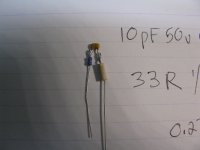
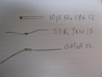
Then I tried swapping out the other Fliege notch op amp, the leftmost one with the 0.047uF from output to inverting input (both Fliege op-amps now the LME49990 again). Oscillation! Boatloads of it, photos below. About 375mV p-p at 11.1MHz. Then I tried adding the datasheet LRC network (33R + 10pF + 0.27uH) first to the output of the leftmost op-amp, then another to the rightmost one. No change in the oscillation at all. Same amplitude, same frequency. National's "mystery" output compensation network, whatever it was intended to fix, doesn't fix this problem.
Photos:
* The first photo 3951 shows the rightmost THS4031 removed and replaced with a LME49990 again.
* The next 3952 shows the result (notch well bottom), essentially the same as before with the two THS4031s installed. This is on 20mV/div again on the scope with the notch filter output going through the 18.3x voltage gain stage, as per the post above.
* The next 3 are an oscillation check. Here the input to the Fliege notch filter is disconnected (that leftmost BNC unhooked), leaving the on-board 49.9R to ground on the input. The bottom blue trace is still the output of the notch filter, run through the 18.3x voltage gain stage. The upper yellow trace is the signal generator, but that isn't going anywhere right now. It is just the bottom blue trace here that matters, looking for oscillation.
All 3 photos are with 20mV/div vertical on the scope. The first photo 3954 is with a 200uS time base, the second with 10mS, and the third with 2uS. No oscillation anywhere. Again, this is a THS4031 for the left op amp and a LME49990 for the rightmost.
* The next two, 3958 and 3959 just show the notch filter still works correctly with the THS4031 + LME49990 pair. This is 2Hz off the notch center in each direction (one is 999Hz and the other 1002Hz), plus run through the 18.3x voltage gain stage.
* The next one shows the leftmost THS4031 now swapped back to a LME49990. Then the next two show the result (bottom blue trace) - oscillation! In that last photo I've now switched over to using just one channel on the scope to get a better look at the oscillation, with the notch filter + 18.3x gain going to the single yellow trace. On this particular scope going single channel doubles the sample rate. 376mV p-p according to the scope, and 1.8div * 50nS/div = 11.1MHz.
*
Hey guys, thanks for the comments! I'll read through tomorrow (midnight here now).
So now that V3.0 works well with the THS4031 chips I couldn't resist swapping the LME49990 back in, one at a time, to see what happens. I also wanted to try out that LRC output compensation network the LME49990 datasheet shows.
The results: swapping out IC4 in the schematic (the rightmost Fliege notch op-amp, the one driving the trimmer pot) from THS4031 to LME49990, it (still) works! Pictures below. No oscillation, but no change in notch depth either. No worse or no better. I've been hoping the LME49990 would be slightly better than the THS4031, in notch depth and/or THD.
Then I tried swapping out the other Fliege notch op amp, the leftmost one with the 0.047uF from output to inverting input (both Fliege op-amps now the LME49990 again). Oscillation! Boatloads of it, photos below. About 375mV p-p at 11.1MHz. Then I tried adding the datasheet LRC network (33R + 10pF + 0.27uH) first to the output of the leftmost op-amp, then another to the rightmost one. No change in the oscillation at all. Same amplitude, same frequency. National's "mystery" output compensation network, whatever it was intended to fix, doesn't fix this problem.
Photos:
* The first photo 3951 shows the rightmost THS4031 removed and replaced with a LME49990 again.
* The next 3952 shows the result (notch well bottom), essentially the same as before with the two THS4031s installed. This is on 20mV/div again on the scope with the notch filter output going through the 18.3x voltage gain stage, as per the post above.
* The next 3 are an oscillation check. Here the input to the Fliege notch filter is disconnected (that leftmost BNC unhooked), leaving the on-board 49.9R to ground on the input. The bottom blue trace is still the output of the notch filter, run through the 18.3x voltage gain stage. The upper yellow trace is the signal generator, but that isn't going anywhere right now. It is just the bottom blue trace here that matters, looking for oscillation.
All 3 photos are with 20mV/div vertical on the scope. The first photo 3954 is with a 200uS time base, the second with 10mS, and the third with 2uS. No oscillation anywhere. Again, this is a THS4031 for the left op amp and a LME49990 for the rightmost.
* The next two, 3958 and 3959 just show the notch filter still works correctly with the THS4031 + LME49990 pair. This is 2Hz off the notch center in each direction (one is 999Hz and the other 1002Hz), plus run through the 18.3x voltage gain stage.
* The next one shows the leftmost THS4031 now swapped back to a LME49990. Then the next two show the result (bottom blue trace) - oscillation!
In that last photo I've now switched over to using just one channel on the scope to get a better look at the oscillation, with the notch filter + 18.3x gain going to the single yellow trace. On this particular scope going single channel doubles the sample rate. 376mV p-p according to the scope, and 1.8div * 50nS/div = 11.1MHz.*
Attachments
-
 IMG_3951.JPG685.1 KB · Views: 59
 -
 IMG_3952.JPG533.4 KB · Views: 53
 -
 IMG_3956.JPG477.2 KB · Views: 50
 -
 IMG_3955.JPG540.2 KB · Views: 48
 -
 IMG_3954.JPG595.2 KB · Views: 52
 -
 IMG_3958.JPG549.9 KB · Views: 96
 -
 IMG_3959.JPG558.9 KB · Views: 48
 -
 IMG_3960.JPG676.9 KB · Views: 51
 -
 IMG_3962.JPG539.5 KB · Views: 61
 -
 IMG_3964.JPG619.3 KB · Views: 55
Last edited:
LME49990's swapped in, plus National's output compensation nework, part 2
Part 2 of the above post, ran out of photo slots again.
* 3965 is a close-up of the oscillation. A somewhat-distorted sine wave.
* 3966 and 3967 show building the ouput compensation network. These are the exact values that National shows in the LME49990 datasheet. 3968 shows the network installed between the output and ground for the left-most Fliege notch op-amp. Lol, when I put that hole JP7 on the chip output line this test is what I had in mind.
* ...and the result in 3969. Same oscillation. No change at all in amplitude or frequency. That compensation network didn't hit a nerve. You can see the compensation network installed in the photo. The notch filter input is still disconnected, of course.
* The next two photos show another copy of the network installed between the output and ground for the right-most op-amp. National's network is now on both op-amps. The result is in 3972: same oscillation. No improvement of any kind.
So.. I'm back to having no idea at all why the LME49990 op-amps here don't work in the Fliege notch filter, but the THS4031 do. Interesting that one LME49990 + one THS4031 did work, but two LME49990 didn't. Either the leftmost op-amp position is the one with problems or there is some odd feedback/oscillation going on between the two LME49990 chips, when both are used.
I guess if I was going to mess with it further the next thing to try would be adding 20R to so in series with the output of each op-amp, to help isolate output capacitance, figuring that might be a likely cause. But series output resistors may affect the notch frequency or depth (haven't tried to simulate it yet). Since the THS4031 works there isn't much reason to continue trying to get the LME49990 to work, especially since it is now officially discontinued by National.
The thing I would like to see now would be the results with that AD8397 dual chip.
Attachments
Last edited:
I'm just thinking about my own options for notch filter etc.
What are your design objectives here? Is notch depth really a critical parameter? Or is that just a convenience to avoid needing to apply inverse of notch freq response to the distortion products when calculating THD?
Have you considered passive notch at all? Was some discussion on the in the great big low distortion oscillator thread. I'm thinking about doing a layout with 2x attenuator, passive notch and 20x gain amp. Don't want to pollute your thread but just thinking about design options for my own very similar project and thought some discussion might benefit all ...
Hello hochopeper,
Your remarks are relevant.
In definitive, the if you want a usable notch filter to allow very low THD level measurements, the notch depth must be good (-60dB), but not very depth nor sharp (Q factor).
If depth or Q is high, the attenuation level will vary much in time because of thermal drift. It will be also very hard to lock the twin-T notch frequency to your oscillator frequency ! (any Hertz difference could change much level).
Adding some gain after the notch is not necessarily a good idea.
You must work with very low level before to analyse it or then you will produce THD by amplifying it.
The Twin-T filter purpose is to remove fundamental and then allow your ADC in your sound card (or others equipments) to measure signal level much lower, while avoiding your ADC to produce THD itself.
To test my oscillator where THD level is about -130dB, i used a passive notch filter with an OPAMP as follower (OPA627).
So, the signal level at OPAMP input remain in mV range and don't introduce measurable THD.
So, you mustn't forget when you perform an FFT measurement you'll need to correct slightly the harmonics amplitude to compensate the filter attenuation at these frequencies.
agdr,
You would try to help finding the issue, could you post your last schematics with actual configuration and all your improvements and changes made ?
You must be careful about OPAMP instabilities when driving capacitive load.
It's a generally a bad idea to use OPAMP output to drive directly a BNC (and it's output coaxial câble). The datasheet of the LME49990 say that the limit is only 100pF...That give only 1 meter of RG58 cable !
SO, if it's not already the case, i suggest you to add 50 Ohms in serie at the output of the last opamp before to drive the BNC
Regards.
FRex
I'm just thinking about my own options for notch filter etc.
What are your design objectives here? Is notch depth really a critical parameter? Or is that just a convenience to avoid needing to apply inverse of notch freq response to the distortion products when calculating THD?
Have you considered passive notch at all? Was some discussion on the in the great big low distortion oscillator thread. I'm thinking about doing a layout with 2x attenuator, passive notch and 20x gain amp. Don't want to pollute your thread but just thinking about design options for my own very similar project and thought some discussion might benefit all ...
I am sure you are familiar with these links?
http://www.diyaudio.com/forums/equi...-twin-t-notch-filter-distortion-analysis.html
Active Twin-T notch filter
Sorry about the delayed reply here! Some unexpected things came up, along with a couple of other project threads going on.
Turbon - I saw your post in the headphone thread - thanks for letting me know the parts made it through the mails.
marce - post #45 - thank you for the additional information and clarification there! Also for those helpful links. So the notching issue comes up with high speed - really high speed. I'm glad you quantified the capacitance involved too, 0.1pF, I've been meaning to try and look up the amount somewhere. Yep that won't make a hill of beans difference at audio frequencies.
hochopeper - good questions. I don't have any really stringent goals for this one, other than to remove as much of the fundamental being applied to the device under test as I can (cleanly, anyway, without loading a lot of extra noise and THD onto the output of the DUT) before going into an analyzer.
So absolute deepest notch might not be the "winner" if it the result isn't as "clean" as a less-deep and/or less wide notch. Good comment above previously about the THD4031 possibly introducing distortion. I was worried about that from the datasheet. Would be kind of counterproductive if the notch filter added amounts of THD to the output of the DUT that were comparable to what the DUT was producing.
As for passive notch filters, I haven't really explored them just under the assumption the notch depth would be (potentially a lot) less, plus there would be insertion loss. But hey, if they are relatively THD free... might be something to consider. I've avoided the Twin-T due to the problems that TI noted in real-world implementations on the 3rd page (their page 20) of that Fliege notch filter white paper here:
www.ti.com/lit/an/slyt235/slyt235.pdf(opens PDF)
Your 20x post-amplifier would solve the insertion loss problem and could likely be made more linear than an active filter.
Frex - good comments! Hey I would be really interested in your thoughts about the Twin-T vs. those TI comments in the link above. One of TI's concerns seemed to be lack of easy variability of the frequency, took 3 part variations if I'm remembering right. I will post a revised schematic. I think the only thing that changed were the chip substitutions, but I'll check. I do have a 49.4R in series with the output BNC. Yeah that LME49990's (direct) capacitive driving ability isn't much. I agree it likely wouldn't do well driving coax directly without some series output resistance like that.
Even though the LME49990 is discontinued and the THS4031 works, part of me would still like to solve this, just for curiosity sake! There is probably a design lesson to be learned here in solving this that might be useful in other stuff in the future. I had another thought after making that post. I believe some op amps out there have an issue of needing a certain amount of resistance in series with the inputs or they will oscillate. Seems that I remember the AD797 being that way, but I'm not finding the mention in a quick look at the datasheet again just now. Maybe that is an issue. Or as was previously posted something about the input bias cancellation circuits fighting/interacting when the two LME49990s are used. That would explain why it works with only one LME49990 and one THS4031.
Lol, even though it means more chip swapping what I really should do is test the other case where the leftmost chip is a LME49990 and the rightmost is a THS4031 and see if that works or oscillates. That test would help narrow it down to a problem with two LME4990s at once (input bias cancellation circuit!) or something with this specific (Fliege) circuit configuration.
AR2 - Dick was certainly one of the best! He will be sorely missed around here.
Turbon - I saw your post in the headphone thread - thanks for letting me know the parts made it through the mails.
marce - post #45 - thank you for the additional information and clarification there! Also for those helpful links. So the notching issue comes up with high speed - really high speed. I'm glad you quantified the capacitance involved too, 0.1pF, I've been meaning to try and look up the amount somewhere. Yep that won't make a hill of beans difference at audio frequencies.
hochopeper - good questions. I don't have any really stringent goals for this one, other than to remove as much of the fundamental being applied to the device under test as I can (cleanly, anyway, without loading a lot of extra noise and THD onto the output of the DUT) before going into an analyzer.
So absolute deepest notch might not be the "winner" if it the result isn't as "clean" as a less-deep and/or less wide notch. Good comment above previously about the THD4031 possibly introducing distortion. I was worried about that from the datasheet. Would be kind of counterproductive if the notch filter added amounts of THD to the output of the DUT that were comparable to what the DUT was producing.
As for passive notch filters, I haven't really explored them just under the assumption the notch depth would be (potentially a lot) less, plus there would be insertion loss. But hey, if they are relatively THD free... might be something to consider. I've avoided the Twin-T due to the problems that TI noted in real-world implementations on the 3rd page (their page 20) of that Fliege notch filter white paper here:
www.ti.com/lit/an/slyt235/slyt235.pdf(opens PDF)
Your 20x post-amplifier would solve the insertion loss problem and could likely be made more linear than an active filter.
Frex - good comments! Hey I would be really interested in your thoughts about the Twin-T vs. those TI comments in the link above. One of TI's concerns seemed to be lack of easy variability of the frequency, took 3 part variations if I'm remembering right. I will post a revised schematic. I think the only thing that changed were the chip substitutions, but I'll check. I do have a 49.4R in series with the output BNC. Yeah that LME49990's (direct) capacitive driving ability isn't much. I agree it likely wouldn't do well driving coax directly without some series output resistance like that.
Even though the LME49990 is discontinued and the THS4031 works, part of me would still like to solve this, just for curiosity sake!
There is probably a design lesson to be learned here in solving this that might be useful in other stuff in the future. I had another thought after making that post. I believe some op amps out there have an issue of needing a certain amount of resistance in series with the inputs or they will oscillate. Seems that I remember the AD797 being that way, but I'm not finding the mention in a quick look at the datasheet again just now. Maybe that is an issue. Or as was previously posted something about the input bias cancellation circuits fighting/interacting when the two LME49990s are used. That would explain why it works with only one LME49990 and one THS4031. Lol, even though it means more chip swapping what I really should do is test the other case where the leftmost chip is a LME49990 and the rightmost is a THS4031 and see if that works or oscillates. That test would help narrow it down to a problem with two LME4990s at once (input bias cancellation circuit!) or something with this specific (Fliege) circuit configuration.
AR2 - Dick was certainly one of the best! He will be sorely missed around here.
Last edited:
QA401 with notch measures oscillator to -130
Using Notch Filters to Improve THD Measurements - QuantAsylum
Using Notch Filters to Improve THD Measurements - QuantAsylum
QA401 with notch measures oscillator to -130
Wow!
I had completely missed that QA blog post. Thank you for the link! I had been using a link to the post following it, about the Q401 status, and hadn't tried bringing up the whole blog page in a awhile. Lol, I just took a look the date of the first post in the thread here. Dec 22, two days after that blog post. Talk about timely. It was the QA401 coming out that reminded me in the first place about this unfinished (oscillating with the LME49990s) Fliege notch board I had posted V1.0 last year.Even more, reading through that blog post, they are using a notch of -50dB, which this V3.0 appears to be doing right now with the THS4031 chips (somewhere around -52dB). AND he is following it with a 20 dB post-amplifier, just like what is on this V3.0 board (although I've been running it at +26dB).
Good grief. I should have bought a powerball lottery ticket. Hmmm..... that diagram they give of the twin-T is using OPA1612's. In re-reading the TI Fliege notch filter app note a few more times I think I mis-understood the need for a 100MHZ GBW op-amp here. The real crition they give is a GBW around 100x of the notch frequency. They just came up with 100MHz because they were running their notch filter at 1MHz as one of the notch frequencies. That explains why the THS4031 has been working just fine with a GBW well below 100MHz at the output voltage swing levels being used.
Since the highest I intend to go is an 11KHz notch a minimum 11 x 100 = 1.1MHZ GBW op amp should be fine, which means most of the op amps out there, including the OPA1611 single version of the OPA1612 (or the OPA209 that was suggested in a post above). A lower GBW op amp should help with avoiding oscillation problems too. I'm going to get some OPA1611 chips and see if those work in the V3.0 board. The OPA1611 THD and noise numbers look better than the THS4031. Comparing the datasheet voltage and current noise density graphs the THS chip goes above 2 at around 800 Hz, while the OPA chip crosses the line at around 20Hz. The THS chip appears to be an ADSL line driver or such with high output current that really shouldn't be needed in this application. The OPA1611 runs on +/-15V supplies too, unlike the AD8397.
Last edited:
OPA1611s oscillate the same way the LME49990s do!
Well as luck would have it I had some OPA1611s on hand. I've just swapped out the two op amps in the V3.0 Fliege notch filter and... oscillation! Very similar to what happened with the two LME49990s in the circuit. Photos below. I removed those two LME49990 datasheet output networks before soldering in the OPA1611 chips.
OK, I think that I know what is going on here. It is simply a phase margin problem. The LME49990 datasheet is one of the few I've seen without an open loop gain/phase plot in it. But I've been studying the THS4031 phase plot vs. the OPA1611 and there is a huge difference. I think to make this thing work with op amps other than the THS4031 it may be necessary to develop a math model for the Fliege and potentially add a zero to cancel a pole somewhere, hopefully without messing with the notch.
At this point I would say go with the Twin-T! If I'm right about a phase margin problem here the Fliege notch filter may wind up being more part-specific to iimplement. The various posts I've seen about the twin-T don't seem to be running into these stability problems in using different op amps. Otherwise, if you are implementing a Fliege notch filter, stay with the THS4031!
Photos:
* The first two are the OPA1611's swapped into the Fliege notch circuit.
* The next two show the oscillation. This is with the filter input BNC disconnected, so 49.9R to ground on the input. The filter output is still going through the 18.3x voltage gain output amplifier here. The frequency appears to be around 16.7MHz. The amplitude is 200mV p-p / 18.3 = 11mV p-p.
Attachments
Last edited:
Wow!
Hahah I thought it was that blog post that motivated you to start this thread. Never realised they were independent.
QA401 with notch measures oscillator to -130
It was this that prompted me to consider a few posts in the low distortion oscillator thread regarding measurements at and around that level where there was some discussion of how the active notch filter and even passive component selection became significant to measurements at or around this level of distortion. Samuel Groner and I think Audio Precision in evaluating their latest units went for a passive notch for ultimate performance. There are some posts floating around of his discussing this, mostly in the low distortion oscillator thread.
I've been idly wondering about that decision vs Dick Moore's comments on the link that AR2 posted:
The Twin-T filter
I needed a way to measure very low levels of distortion that was easy and relatively cheap. I wasn't ready then to buy a high-precision THD analyzer or a wave analyzer -- I thought I could cheap out. Years ago I had built a passive Twin-T notch filter tuned to 1kHz to make quick and dirty measurements of amps and oscillators. The Twin-T is the most attractive notch filter from a performance point of view -- it can (with care) be tuned for a notch depth of over 100dB, though the tuning process is a little (!!!) finicky. The trouble is, a) they are hard to tune over a range of frequencies, b) they require numerous adjustable parts for best performance, and c) they attenuate the harmonics of interest to varying degrees, so that you can't easily make a level measurement with an AC voltmeter or scope and know how much correction factor to apply.
The typical passive Twin-T filter attenuates the 2nd Harmonic of the tuned frequency by about 9.4dB. That's a lot, and the 3rd H. is attenuated by over 5dB. Accounting for variations in just those two harmonics alone makes precision measurements impossible. The reason for this is that although the notch of the twin-t is very deep, the filter's bandwidth at the -3dB points is too wide; in other words, the Q is too low. Clearly, some form of sharpening of the filter's frequency band is needed.
It is surely inconvinient to accurately characterise a passive notch filter frequency response and do some math after taking the measurement but ... I think I'll try the passive notch approach.
I notice here - File Downloads - that there is QA401 software available now for beta testers of the unit. Was told a few weeks back by email that they were waiting on anodizing of enclosures still ... I'm keen to get a hold of one soon!
Chris
hochopeper - when I first read that QA blog post it was so similar my first thought was "geezzz - someone at QA must have seen this thread and did a general post about notch filters". But then I checked the posting dates and realized it was the other way around! Their blog post was first. Talk about crazy coincidences.
That is interesting info about the width of the passive twin-T notch well. Yeah that is a lot of attenuation at the 2nd and 3rd. I think in Rod Elliot's information this Fliege notch was supposed to be down only 0.1dB or so at the 2nd. But...if the result of the passive twin T is exceptionally clean - which it probably will be - it is certainly worth considering. If you build it please post the results!
Good to see that QA401 software link. I'm going to get one too, despite my wishes that they hadn't used USB power again. For just the $430 or so it should be a useful upgrade/replacement to the QA400.
Last edited:
- Home
- Design & Build
- Equipment & Tools
- Fliege 1kHz notch filter project PCB