Candidate Conceptual F6 schematics; maybe?
Got three of them. Their base schematics are those shown in the article by Mr. Pass which is entitled: "The Zen Variations-Part 2; The Penultimate Zen's Current Sources. The attached file is ConceptualF6#0. I added a large bypass capacitor across R1, a blocking capacitor C2' at the collector of ZTX550, and of course the Jensen transformer. I hope that I got the phasing of the signals correctly on the secondaries.
Got three of them. Their base schematics are those shown in the article by Mr. Pass which is entitled: "The Zen Variations-Part 2; The Penultimate Zen's Current Sources. The attached file is ConceptualF6#0. I added a large bypass capacitor across R1, a blocking capacitor C2' at the collector of ZTX550, and of course the Jensen transformer. I hope that I got the phasing of the signals correctly on the secondaries.
Attachments
Candidate F6 schematics; maybe?
Here is the second one ConceptualF6#1.pdf: I believe my additions to the basic skeleton are clear, and I have the correct signal phasing on the transformer secondaries.Got three of them. Their base schematics are those shown in the article by Mr. Pass which is entitled: "The Zen Variations-Part 2; The Penultimate Zen's Current Sources. The attached file is ConceptualF6#0. I added a large bypass capacitor across R1, a blocking capacitor C2' at the collector of ZTX550, and of course the Jensen transformer. I hope that I got the phasing of the signals correctly on the secondaries.
Attachments
Candidate F6 schematics; maybe?
The third schematic is ConceptualF6#2.pdf which is a Jensen transformer-coupled Aleph current source. Use JFETs instead of MOSFETs in the three candidate schematics so as to be commensurate with Conceptual F6 methodology.Here is the second one ConceptualF6#1.pdf: I believe my additions to the basic skeleton are clear, and I have the correct signal phasing on the transformer secondaries.
Attachments
Nelson:
I am trying to understand the mechanism of the secondary loading on the harmonics. With the Jensen JT-123-FLPCH I haven't been able to detect a significant effect from secondary loading.
I am trying to understand the mechanism of the secondary loading on the harmonics. With the Jensen JT-123-FLPCH I haven't been able to detect a significant effect from secondary loading.
You are overlooking another location for trimming the cancellation, which is
resistance across the secondary coils. Typical values would be on the order
of 200 ohms or more.

Makes divider with gate stopper?
nope
just resistor across secondary,creating constant load
same as you walking with or without sack of cement on your shoulder(s)
or constant felt brake under EMT927/930 platter

Wouldnt altering the resistance/impedance of the secondary affect the reflected impedance and thus voltage ratio/amplification factor, changing the gain sligjtly. Similar to what Zen pot does on output. Dunno,just guessing.. Gotta go lay baby girl down.. sweet dreams!
loading secondary will decrease amplitude
so , speaking of directly altering modulation of gate , not influencing xconductance shape , as with ZAP
Last edited:
nope
just resistor across secondary,creating constant load
Of course, gate stopper is negligible in front of high Z gate.
I am stupid.

I used the word gain and that was wrong as i did not mean gain of the output stage but of the transformer, which would have amplification of less than 1.nope
just resistor across secondary,creating constant load
same as you walking with or without sack of cement on your shoulder(s)
or constant felt brake under EMT927/930 platter
loading secondary will decrease amplitude
so , speaking of directly altering modulation of gate , not influencing xconductance shape , as with ZAP
I have tried that. I still cannot see a significant difference. I am trying to understand the physical mechanism that secondary loading has w.r.t. distortion.
load/unload two secs differently
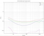
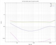
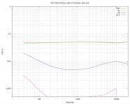
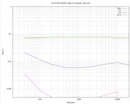
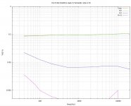
Here are actual measurements of the circuit shown in #2213 with a variety of adjustments to the Zen pots P3 and P4. The "spare" primary winding is modulated at 0.8*Vout.
Attachments
-
 F6-PCB2-Rs0R12-Gain-5-Txmod2c-Zen-075.jpg157.6 KB · Views: 275
 -
 F6-PCB2-Rs0R12-Gain-5-Txmod2c-Zen-080.jpg152.6 KB · Views: 269
 -
 F6-PCB2-Rs0R12-Gain-5-Txmod2c-Zen-103.jpg151 KB · Views: 259
 -
 F6-PCB2-Rs0R12-Gain-5-Txmod2c-Zen-130.jpg149.9 KB · Views: 261
 -
 F6-PCB2-Rs0R12-Gain-5-Txmod2c-Zen-170.jpg149.5 KB · Views: 253
I haven't listened yet. I am now modifying the 2nd channel to match.
Which do you like best?
I experimented with adjustments to the other PCB which still has the primary windings in parallel. For Gain other than 2.0, I could not obtain distortion spectra comparable to those in post #2237 which has the "spare" primary winding modulated by 0.8*Vout.
If anyone is interested, I can offer an explanation for why the modulation is optimal at (Gain-1)/Gain*Vout.
If anyone is interested, I can offer an explanation for why the modulation is optimal at (Gain-1)/Gain*Vout.
- Home
- Amplifiers
- Pass Labs
- F6 Amplifier