Is capacitor coupling acceptable? The direct coupling you show at the primary will not influence potential DC offset at the output.
I am not familiar with LTSPICE. Please jot down: voltage of power rails, current flowing through each JFET, and the maximum power output into 8 and 4 Ohm loads.
Can one have multiple upper and multiple lower JFETs to increase power?
The rail voltages are defined by ".param vpwr=25 vrip=.0". The output fet bias current is 1.3A. Max output power into 8 ohms is 25 watts, as with the F5.
Multiple input JFETs might improve the drive of the transformer primary. I estimate that the single pair of complementary JFETS shows with have a output impedance of about 15 ohms.
Not necessarily simple, Ilquam, but do not undetstimate the circuit JG posted and ZM eluded to.
I cannot see a connection between the schematic in post 706 http://www.diyaudio.com/forums/pass-labs/216616-f6-amplifier-71.html#post3121887 and the F6. What am I missing?
Post 693 & 4. Leading to this as possible candidate for guilded Lily FE.
http://www.diyaudio.com/forums/pass-labs/161411-buffer-preamp-shunt-ps-7.html#post2558131
Post #68
http://www.diyaudio.com/forums/pass-labs/161411-buffer-preamp-shunt-ps-7.html#post2558131
Post #68
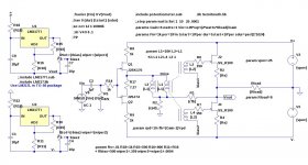
Here is an F6 variant using LM317L voltage regulators instead of batteries. The parts count is sorta high, but it might be possible to reduce it somewhat. I make no claim that the resistor and capacitor choices are optimal, but it simulates well. Output FET bias current 1.3A, 25V rails.
Attachments
You could make the whole F6 out of LM317/337. Both the input buffer and as ouitput-devices. The act as quite slow depletion.mode devices... I have several of each at home... I want to try it.
Johannes.
Circlomanen: Please share with us a simplified schematic of the underlined. Best regards.
With enough monkeys on typewriters for long enough we will design all of the future works of Nelson Pass.
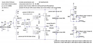
Here is another F6 bias circuit design using zener diodes instead of batteries or voltage regulators. The component count is somewhat smaller, and it simulates well.
Here is another F6 bias circuit design using zener diodes instead of batteries or voltage regulators. The component count is somewhat smaller, and it simulates well.
Attachments
C7 and C1 ?
C7 and C1 should probably be increased to around 10uf, maybe more depending on the transformer parasitic coupling.

I'm more concerned with dynamic gate AC current demands , which will be superimposed with DC bias potential
remember that those are small signal xformers
better find a way to disconnect them from DC path
I do not understand what the problem is. In the case of the lower fet, the cap is from the negative rail to the bias voltage on the opposite end of the winding from the lower fet gate. In the case of the top fet, the cap is from the amp output to the bias voltage on the opposite end of the winding from the upper fet gate.
The voltage on the gate relative to the bottom of the source resistor is the DC bias voltage PLUS the AC voltage across the secondary winding. No DC current flows thru the secondary (expect for gate-source leakage current on the order of one uA).
What am I missing?
Last edited:
ok
maybe I'm too hysteric regarding DC through coil (even in range of uA) , but another thing which bugs me is possible variable loading of secondary,due to variable impedance of gate itself and very possible not enough loading ;
if you put secondary coil as you want , AC path will be gate-sec-C1(C7)-bottom of Rs
Rg ignored
if you connect wiper to gate and sec in series to C1(C7) , AC path will be (primary) in more uniform way - bias net-C1(C7)-sec-bottom of Rs
bias net represent both lower and more uniform loading than gate
that way there will not be any trace of DC through coil and loading of sec will be more uniform in freq. domain
from experience - I know that sole worse thing than unloaded secondary is just heaven fallen on your head
ask Vikings
use highish value of trimpot , to avoid too much loading of secondary , or insert at least few K resistor in series with wiper
Last edited:
With enough monkeys on typewriters for long enough we will design all of the future works of Nelson Pass.
Here is another F6 bias circuit design using zener diodes instead of batteries or voltage regulators. The component count is somewhat smaller, and it simulates well.
Cool stuff. Some questions please if you don't mind:
a) What is the purpose of C8 for the top fet and why do we not have it in the bottom fet ?
b) Sorry am not good at reading sim results, but what is the gain you see Open Loop (AOL) and then Close Loop (ACL) (also what is R1 and R2 for close loop case). Does varying the bias circuit from battery, LM317 and then zener cause changes to ACL and AOL ?
Many thanks and great work !
ok
maybe I'm too hysteric regarding DC through coil (even in range of uA) , but another thing which bugs me is possible variable loading of secondary,due to variable impedance of gate itself and very possible not enough loading ;
if you put secondary coil as you want , AC path will be gate-sec-C1(C7)-bottom of Rs
Rg ignored
if you connect wiper to gate and sec in series to C1(C7) , AC path will be (primary) in more uniform way - bias net-C1(C7)-sec-bottom of Rs
bias net represent both lower and more uniform loading than gate
that way there will not be any trace of DC through coil and loading of sec will be more uniform in freq. domain
from experience - I know that sole worse thing than unloaded secondary is just heaven fallen on your head
ask Vikings
use highish value of trimpot , to avoid too much loading of secondary , or insert at least few K resistor in series with wiper
How about this?
Attachments
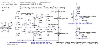
Cool stuff. Some questions please if you don't mind:
a) What is the purpose of C8 for the top fet and why do we not have it in the bottom fet ?
b) Sorry am not good at reading sim results, but what is the gain you see Open Loop (AOL) and then Close Loop (ACL) (also what is R1 and R2 for close loop case). Does varying the bias circuit from battery, LM317 and then zener cause changes to ACL and AOL ?
Many thanks and great work !
a) The bias for the bottom fet is easy. All that is needed is to generate a stable voltage relative to the bottom rail using power from ground.
The source and gate of the top fet are moving with Vout the output voltage. The average voltage of the output is zero. By placing an RC filter (R18 and C8) between V+ and Vout we establish about 14 volts across C8 to provide bias current through the zener diode.
b) With Gain=6, the spice statement ".param rpd=10 rfb=(Gain-1)*rpd" gives R2=10 ohms, and R1=50 ohms.
With the source resistors Rs near zero, the open-loop gains is 100.
With the source resistors Rs=.1 ohms, the open-loop gains is 62.
All of the bias circuits shown produce very similar results.
- Home
- Amplifiers
- Pass Labs
- F6 Amplifier