If you are looking for leaded transformers which work in place of the Jensen, you might also look at the Cinemag CMOQ-4L or CMOQ-4H. The -4H has 80% nickel instead of the 50% of the -4L or the Jensen. This may or may not matter for the F6, but the -4H is actually cheaper than the Jensen and contains more nickel, so seems a good choice. I have a pair on the way at the moment.
If you are looking for leaded transformers which work in place of the Jensen, you might also look at the Cinemag CMOQ-4L or CMOQ-4H. The -4H has 80% nickel instead of the 50% of the -4L or the Jensen. This may or may not matter for the F6, but the -4H is actually cheaper than the Jensen and contains more nickel, so seems a good choice. I have a pair on the way at the moment.
I think more nickel will sound less colored!
Pulled out the distortion analyzer and measured 2nd harmonic on stock configuration and I'm getting -81dB (1W into 8 Ohms)
Once I have had a chance to enjoy listening to the amp in stock configuration, I'll mod one channel by moving cap lead to other side of resistor and redo the measurement
Once I have had a chance to enjoy listening to the amp in stock configuration, I'll mod one channel by moving cap lead to other side of resistor and redo the measurement
The diyAudio F6 PCB was made to the schematic provided by Nelson when asked for one, specifically, this -
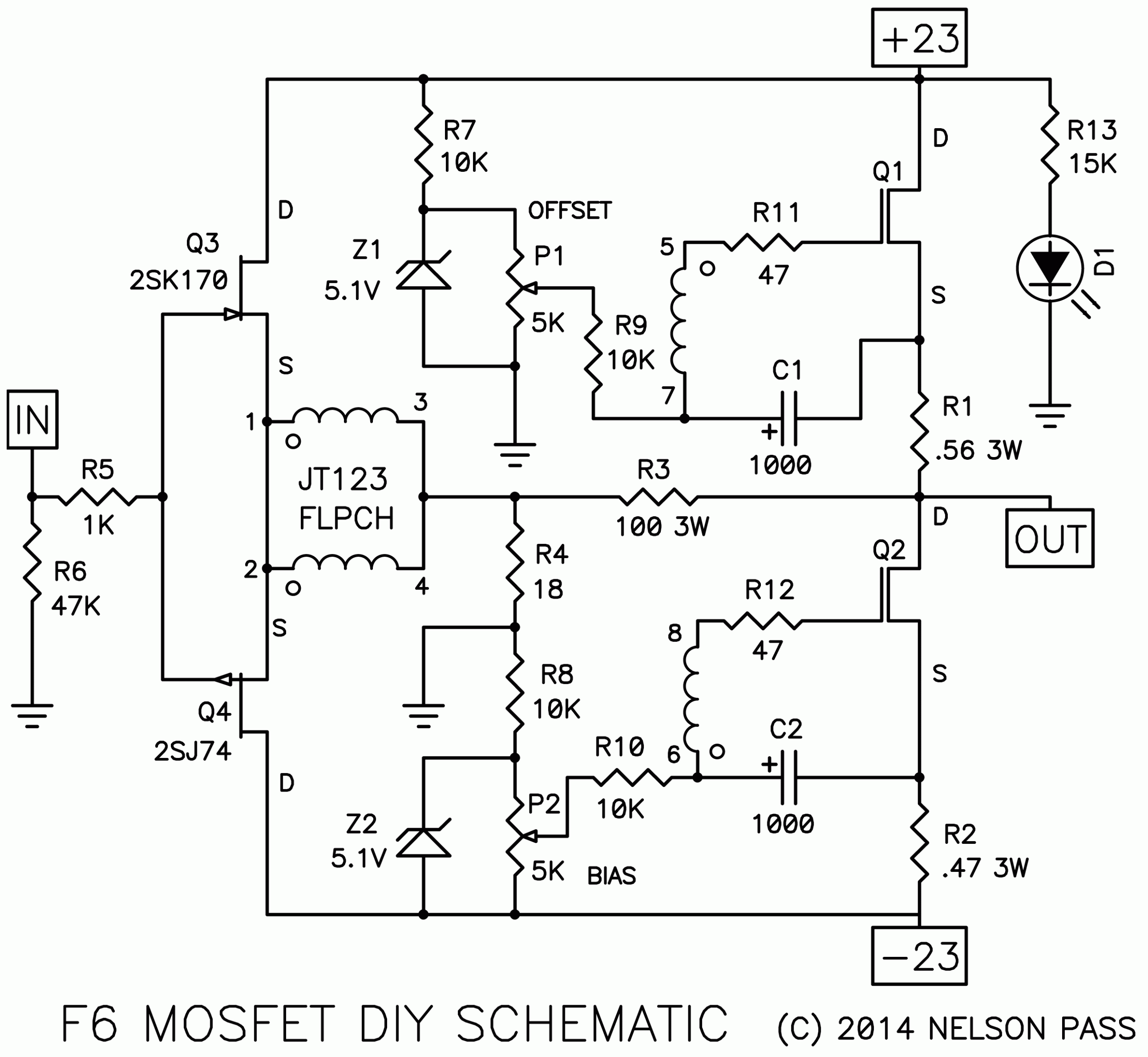
Note that the capacitor is attached directly to the source of the Mosfets.
Yes, it does differ from the "Output Degeneration" schematic from the presentation at BAF '13 -
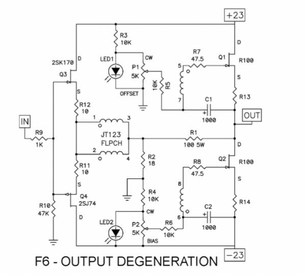
Hi Nelson, is there a reason why you provided a different schematic ("F6 MOSFET DIY SCHEMATIC") to 6L6 which differs from that in your original F6 article ("F6 - OUTPUT DEGENERATION")? Was this done intentionally? Which circuit should we be building? I personally have built the F6 from the store boards and am wondering if I should carry out the mod. Thanks.
One is an example of output degeneration, and the other is an example with
no degeneration from an AC point of view. In both cases, there is
degeneration at DC for bias stability vs temperature and such.
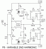
There is a third schematic with pots in parallel with the Source resistors with
the wipers attached to the capacitors so that the amount of AC degeneration
on top and bottom is variable. That one is my favorite.

no degeneration from an AC point of view. In both cases, there is
degeneration at DC for bias stability vs temperature and such.
There is a third schematic with pots in parallel with the Source resistors with
the wipers attached to the capacitors so that the amount of AC degeneration
on top and bottom is variable. That one is my favorite.
Thank you Nelson. If I understand correctly (I am new at this) is that the no degeneration version has predominantly 3rd harmonic distortion, whereas the output degeneration version introduces 2nd harmonic. Adjustable via the output resistors. I think I will try this out and see how it sounds. Thanks again!
I will looking for what you have to say after doing so. I would not think the store would want to change the board from the official one NP released. As Russell said no big deal jumping across the resistor. I assume you are going to just snip the capacitor lead and move it to the other side of the resistor.
Pots would be nice but you need a distortion analyzer of some sort to get the benefit. Quick and dirty (and it works from my mod experience) is to cut traces and jumper and use 0.47 and 0.56 ohm resistors.
The schematic is my release. I did not do the boards.
Since it is Nelson's circuit, why not change the layout to accommodate all mods so builders easily choose which mods to incorporate in their build? At the same time fix the layout so the outputs are symmetrical?
I've attached the circuit with variable 2nd harmonic. However, it has SemiSouth outputs. I assume it can be adapted to use IR parts
Attachments
Last edited:
Yeah. I agree. I don't know why there seems to be so much reluctance to revise existing pcbs.Since it is Nelson's circuit, why not change the layout to accommodate all mods so builders easily choose which mods to incorporate in their build? At the same time fix the layout so the outputs are symmetrical?
I'm of the opinion that boards should allow flexibility in implementation.
You can also achieve 2nd harmonic through selecting devices with different levels of transconductance without modding, but I found my devices are very similar in transconductance (not different enough).Thank you Nelson. If I understand correctly (I am new at this) is that the no degeneration version has predominantly 3rd harmonic distortion, whereas the output degeneration version introduces 2nd harmonic. Adjustable via the output resistors. I think I will try this out and see how it sounds. Thanks again!
I have another idea, never used anywhere that I am aware of (my invention
). I need to test it out first though.Last night I modded my stock DIYaudio "no degeneration" PCB to the "output degeneration" version. I realised that since I am not using input degeneration, only output degeneration, my circuit is now a kind of hybrid of the two circuits posted above. Seems counter-intuitive, although I guess this is what DIY is all about....
Anyways, I can't say I have noticed a huge difference in the sound. I always find it difficult to make before/after comparisons based on auditory memory not being able to A/B. If there is a difference, I cannot say it is significant. Then again, in the article it is mentioned that the distortion spectrum will be somewhat random and dependant on the matching of the MOSFETs, so I guess every F6 probably sounds a little different. Without a distortion analyser it's impossible to really know what's going on.
Anyways, I can't say I have noticed a huge difference in the sound. I always find it difficult to make before/after comparisons based on auditory memory not being able to A/B. If there is a difference, I cannot say it is significant. Then again, in the article it is mentioned that the distortion spectrum will be somewhat random and dependant on the matching of the MOSFETs, so I guess every F6 probably sounds a little different. Without a distortion analyser it's impossible to really know what's going on.
If you cannot hear any or very little difference why worry about it. If you see anything with a scope and distortion analyzer then you would start worrying about something you cannot hear. I played around with the values of the source resistors when I first built my F6 and really could not hear that much if any difference. It might say something about my hearing and others will better hearing could tell a difference. I may be blessed.
Playing around with source resistors has no effect on stock pcb.I played around with the values of the source resistors when I first built my F6 and really could not hear that much if any difference. It might say something about my hearing and others will better hearing could tell a difference. I may be blessed.
My understanding is the stock pcb is made exactly like the circuit Nelson designed with mosfets for diyer's. Are you saying that Nelson designing the circuit with 2 different value source resistors is wrong and has no effect on the sound and could have been designed with the same value resistors as per Mosfet schematic if it does not have any effect on the sound. Or does the circuit board have an error and is not as Nelson designed it with the IRF240 mosfets? The F6 mosfet DIY schematic shows the 1000 uh caps attached between the source and resistor. Is not the diyaudio board made this way?
This is Nelson's comment on the two variations of the schematic. "One is an example of output degeneration, and the other is an example with
no degeneration from an AC point of view. In both cases, there is
degeneration at DC for bias stability vs temperature and such."
So it looks like the DIY boards benefit from DC degeneration (with the 2 different value resistors) but not AC degeneration. If you sim the DIY schematic the harmonics don't change if you have different or equal source resistors, this model has more 3rd harmonic than 2nd harmonic.. I can't speak to what is happening DC wise.If you move the cap lead to the bottom of the source resistors (as the degeneration schematic) then different value source resistors make a difference, making the 2nd harmonic more predominant than the 3rd, this is the AC degeneration happening.For my ears I could hear a difference (better for me) with the AC degeneration,2nd harmonic dominant model.
My understanding is the stock pcb is made exactly like the circuit Nelson designed with mosfets for diyer's. Are you saying that Nelson designing the circuit with 2 different value source resistors is wrong and has no effect on the sound and could have been designed with the same value resistors as per Mosfet schematic if it does not have any effect on the sound. Or does the circuit board have an error and is not as Nelson designed it with the IRF240 mosfets? The F6 mosfet DIY schematic shows the 1000 uh caps attached between the source and resistor. Is not the diyaudio board made this way?
1) To change harmonic content using different source resistors values, the cap lead needs to connect to other side of resistor like in F6 article.
So why did Nelson add 0.56 Ohm and 0.47 Ohm resistors if they do nothing to change harmonic profile.
That had me dumb struck for a while. My best guess on this is, Nelson selected IRFP240 devices with different values of Transconductance to get the 2nd harmonic he wanted. The higher transconductance part he placed on the positive power rail and the lower transconductance part he put on the negative rail.
To compensate for the higher thermal drift of the higher transconductance part he added 0.56 Ohm resistor. That's my best guess on that.
Probably the easiest way to hear the effect of changing 2nd harmonic content on the fly would be to solder cap lead to wiper of potentiometer and adjust potentiometer till your ear is happy.
You would only need to do it on one of the devices it's not necessary to do both devices. Or just reroute cap lead to other side of resistor. Or you can do what Nelson did and carefully select parts with differing values in transconductance.
Last edited:
If I understand this right the diyaudio board they sell is just as the Diy mosfet schematic and no errors are in the board but you think the connection points of the 1000 uh should be changed. The original F6 article specifies the semisouth jfets when the connection points are as you describe but when Nelson designed the circuit with mosfets he decided to change the connection point for the 1000 uh cap. Is this correct.
If I understand this right the diyaudio board they sell is just as the Diy mosfet schematic and no errors are in the board but you think the connection points of the 1000 uh should be changed. The original F6 article specifies the semisouth jfets when the connection points are as you describe but when Nelson designed the circuit with mosfets he decided to change the connection point for the 1000 uh cap. Is this correct.
There are benefits in doing it the way Nelson has done it, but it requires selecting parts of different transconductance.
It would be nice to have the option on the board to connect it both ways though.
So why did Nelson add 0.56 Ohm and 0.47 Ohm resistors if they do nothing to change harmonic profile.
No, I simply made the cap location modification to an existing circuit whose
Source resistors reflected the desire for some 2nd harmonic by different
degeneration top vs bottom.
No, I simply made the cap location modification to an existing circuit whose
Source resistors reflected the desire for some 2nd harmonic by different
degeneration top vs bottom.
Thank you Nelson.
However, without a picture, I'm not certain I understand.
Are you saying your pcb had the option of installing the cap in two different positions.
In the F6 article the circuit presented there, clearly has that effect.
With the existing pcb the cap wiring is connected differently.
Using 0.56 and 0.47 I did not get the expected amount of 2nd harmonic as measured on distortion analyzer. The same thing occurs in simulation.
In simulation, the circuit the pcb is based on, does not respond to changes in source resistance.
My distortion meter also gives much lower 2nd harmonic distortion with this circuit.
I will try just physically tapping another source resistor in parrallel (change source resistance on the fly) to see if 2nd harmonic distortion changes on my meter.
- Home
- Amplifiers
- Pass Labs
- F6 Amplifier