Hmmm... of course this adds complexity, but one could sense the device current, and put an active device around the "bias resistor" sitting on the source, and then slide it into conduction proportionally until it is full on, making the "knee" that was shown essentially disappear (of course it is really just spread over a very huge range...).
A kind of sliding arrangement... NP liked that stuff.
_-_-bear
A kind of sliding arrangement... NP liked that stuff.
_-_-bear
Last edited:
As Patrick said - there is more than one way to skin a cat. As I reiterated
in the Turbo, more current is better as long as you can take the dissipation.
At the same time, I respond to people who complain that 25 watts or
whatever is not enough.
Nelson - thanks for the input, as always.
I went the other direction. With 16V rails I could crank up the amps and keep total device dissipation in check. Ibias=2A through each device. Ipk=4A for peak output of 128W and 64WRMS (I hope I did the calculations correctly).
I love seeing the Turbo. I'm sure I'll build it. For my Balanced amp, I went for the most I could get in Class A without paralleling outputs.
Now, I have to tackle some SITs...
Re: The sharp knee point circled in red is that at which the conduction of the diode becomes prominant.
Patrick
OK. Admittedly, I'm thinking "over my head" on this one, so please don't beat me up too badly in responses......
What if the another diode and resistor (in series) be placed in parallel with the diode in the design? Would this "soften" the sharp knee point by introducing a second knee point to ease the transition? Seems like you could smooth the transition accordingly--if in fact this is a valid concern for the quality of the amp.
Disregard, if this is a mindless suggestion.........
Thanks Salas, if Papa permits i'll put them back in but only then.
Question here, Do the MUR3020's need to go to the main heatsink, or would a clip on or bolt on do, something that could dissipate 5-10W?
...Good question, my reasoning is that it's simpler to bolt them on main heatsink and temperature will the be the same as it's companion transistor....tracking of both will remain constant at all operating temperatures ie: the by now famous "knee" will not shift as operating temperature changes up to stabilization point.
But really it makes for cleaner construction with this PCB.
With my other solution, rectangular PCB for mono-block with the transistors 4 each side it´s easier to implement what you suggest ( more space ) although there again it's cleaner to just bolt everything on main heat sinks.
..That said i'm very keen to hear your input on this PCB.
Increasing first stage gain
This note describes a technique for increasing the open-loop gain of the F5, F5-turbo, or any other amplifier with a similiar first stage with voltage gain. The open-loop gain of the F5 family is the product of the voltage-gain of the JFET input stage with the voltage-gain of the MOSFET output stage. The voltage gain of a stage is the product of the effective transconductance with the load resistance of the stage. Thus we can increase the voltage gain of a stage by increasing its effective transconductance or its load resistance.
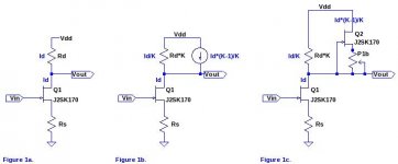
Figure 1a shows a simplified F5 input stage. In the quiescent state (when Vin = 0), Vout(0) must be set to the voltage needed to bias the MOSFET stage for the desired bias current. If the F5 family, trimmer resistors P1 and P2 are adjusted to achieve MOSFET bias current and zero output voltage.
Figure 1b shows how to increase Rd (and the voltage gain) by a factor of K while maintaining the output bias voltage Vout(0). To maintain a constant voltage drop across the Rd*K drain resistor, its current must be divided by a factor of K. The remaining current Id*(K-1)/K is supplied by a constant current source.
Figure 1c shows the implementation of the constant current source using a single JFET and trimmer resistor. The negative side of the F5 input stage is modified similarly.
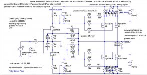
Figure 2 shows a modified F5-Turbo-V2 in which the first stage gains have been increased by factors of 2.75X on the positive side and 3.75X on the negative side. (I need to make adjustments to R6 and R6 to balance to open-loop gains of the two amplifier chains.) I have performed numerous SPICE simulations of this modified circuit and they indicate significant reductions in THD, consistent with the increase in open-loop gain. With the circuit shown, LtSpice reports a THD at 1kHz, 1 watt into 8 ohms of .00055%. Not bad.
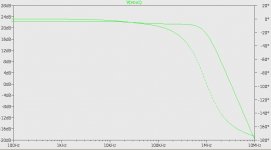
There are two possible issues regarding this modification: thermal stability and bandwidth. My guess is that R21/Th1 and R22/Th2 might need different values to maintain thermal stability. The amplifier bandwidth is reduced since the RC time constant related to Rd and the MOSFET gate capacitance has been multiplied by a factor of K. Figure 3 shows a bode Bode plot of the modified amplifier, in which the bandwidth is still very good and the phase margin is excellent.
This note describes a technique for increasing the open-loop gain of the F5, F5-turbo, or any other amplifier with a similiar first stage with voltage gain. The open-loop gain of the F5 family is the product of the voltage-gain of the JFET input stage with the voltage-gain of the MOSFET output stage. The voltage gain of a stage is the product of the effective transconductance with the load resistance of the stage. Thus we can increase the voltage gain of a stage by increasing its effective transconductance or its load resistance.
Figure 1a shows a simplified F5 input stage. In the quiescent state (when Vin = 0), Vout(0) must be set to the voltage needed to bias the MOSFET stage for the desired bias current. If the F5 family, trimmer resistors P1 and P2 are adjusted to achieve MOSFET bias current and zero output voltage.
Figure 1b shows how to increase Rd (and the voltage gain) by a factor of K while maintaining the output bias voltage Vout(0). To maintain a constant voltage drop across the Rd*K drain resistor, its current must be divided by a factor of K. The remaining current Id*(K-1)/K is supplied by a constant current source.
Figure 1c shows the implementation of the constant current source using a single JFET and trimmer resistor. The negative side of the F5 input stage is modified similarly.
Figure 2 shows a modified F5-Turbo-V2 in which the first stage gains have been increased by factors of 2.75X on the positive side and 3.75X on the negative side. (I need to make adjustments to R6 and R6 to balance to open-loop gains of the two amplifier chains.) I have performed numerous SPICE simulations of this modified circuit and they indicate significant reductions in THD, consistent with the increase in open-loop gain. With the circuit shown, LtSpice reports a THD at 1kHz, 1 watt into 8 ohms of .00055%. Not bad.
There are two possible issues regarding this modification: thermal stability and bandwidth. My guess is that R21/Th1 and R22/Th2 might need different values to maintain thermal stability. The amplifier bandwidth is reduced since the RC time constant related to Rd and the MOSFET gate capacitance has been multiplied by a factor of K. Figure 3 shows a bode Bode plot of the modified amplifier, in which the bandwidth is still very good and the phase margin is excellent.
Attachments
why not v3 , this one is not above the current f5 c boards currently available ...
Yes, same question here
Plus this one operate the input jfets above their rating. No cascoding?
Another idea would be to have some clever set jumpers that allow to use the diode places for more power fets. I have no clue about pcb design. It's just an idea. Good for those that want to reduce the value of source resistors (I used 0,22 ohms in my F5X) instead of using diodes.
Last edited:
anything that can be brought in
combine #8689 and #12042
Yes, same question here
Plus this one operate the input jfets above their rating. No cascoding?
Another idea would be to have some clever set jumpers that allow to use the diode places for more power fets. I have no clue about pcb design. It's just an idea. Good for those that want to reduce the value of source resistors (I used 0,22 ohms in my F5X) instead of using diodes.
I'll have a look at that although my worry is that the heatsink may have trouble dissipating the heat from 4 power FETS per rail.
Perhaps the Diodes could be moved.
Anybody have an idea of the maximum dissipation we can expect through the diodes on the F5 v3?
i'll look at the possibility of some wire links to jumper out the diodes.
I've added some keystone compact test points to make setup easier.
Andy
- Status
- This old topic is closed. If you want to reopen this topic, contact a moderator using the "Report Post" button.
- Home
- Amplifiers
- Pass Labs
- F5 Turbo is posted