While testing, remember to short the input out completely - junction of jfet gates to be routed to ground. This will stop the jfets conducting and make troubleshooting marginally easier. You cannot set bias in this condition, for that you have to short the input pads of the board.
Ok just a point there, when I test there is nothing on the input, in fact not even connected to anything yet. I don't short it out at all. Would this affect the readings?
how about the other channel board? in the unpowered state anything I can test to compare the two boards?
Hi,
If the input is open and the source resistor is present it is the same as applying full bias. Which means you will typically measure 0 or close to zero across the FET as it fully conducting. The only way to pinch off the bias is to completely short out the Vgs, so the jfet stops conducting.
For bias setting we normally keep the input shorted as the three resistors around the gate and source are enough to fully bias the outputs at idle signal condition. Keeping it open would mean the bias can never go low enough to be properly set.
I still am not convinced that is the core issue though, as you have decent voltage sag with a passive load, and an easy one at that. Would continue to poke around, just to be sure that you got 'em all.
OK so what else can be the culprit?
I guess there is no source resistor there yet as the secondary board where the mosfets and source resistor exist is not installed yet.
I've tested the V across R27/25/29 and they seem to give expected voltages.
what else is there in the half circuit that could eat up all that voltage?
one of the pots? could R7-10 (feedback resistors do it? I pretty much test each resistor before soldering, and that one I'm pretty sure is ok. but would too little feeback cause this, I've upped the R to 200ohm)
The only thing that gets marginally warm when I power it up are the BJT's.
R11/12 and beyond isn't even on the board....
I don't know what else to test for...
Last edited:
Frankly, this is a very weird case. I do hope an idea presents itself soon, because I don't really have any more.
Can you try removing feedback resistors, just lifting one leg would do it. They do connect the two halves of the circuit and cause conduction between them without a ground reference. Worth a try.
Basically the only thing that can cause this is a dodgy or miswired bjt, that's my guess. It is not operating correctly.
without actual mess in front of me , on my desk , I'm lost ........
thing is behaving in way as bjts aren't good ....... as I said - when they have firm potential at bases , emiters must be lower by roughly 0V65 ( in reality anything between 0V57 and 0V7) , whatever load at emiter is
so , if placement ( exact type where intended and pinout) is OK , then bjts are faulty
edit : as output mosfets aren't in circ , feedback resistors are irrelevant ........ same as position/value of pots in bjt colectors
everything must be biased via JFet source resistors
ZM,
what is the mechanism that drops the voltage to nothing with the Jfets inserted. If they were bad, would the bjt's show a different voltage if measured from emiiter to ground, when compared to measuring across the 4.75k voltage divider resistor?(assuming the Vbe drop of around.7V)
what is the mechanism that drops the voltage to nothing with the Jfets inserted. If they were bad, would the bjt's show a different voltage if measured from emiiter to ground, when compared to measuring across the 4.75k voltage divider resistor?(assuming the Vbe drop of around.7V)
ZM,
I'm a little confused at what you are saying.
The base of the BJT is about 41V.
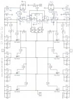
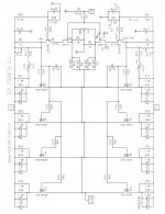
If you look closely at #3012 you can see that there is a trace that connects the BJT emitter to the drain of the jfet.
When testing the drains (without the jfets nor 10k resistor in ) I do get 15.47V.
What I don't understand, is that I thought the point of the BJT is to allow the jfets to operate at a lower voltage. Are you saying that I should get 41V0 - 0V65 at the emitter of the BJT? or perhaps only 16V going into the BJT at the Base, which doesn't seem correct looking at the schematic.
I'm a little confused at what you are saying.
The base of the BJT is about 41V.
If you look closely at #3012 you can see that there is a trace that connects the BJT emitter to the drain of the jfet.
When testing the drains (without the jfets nor 10k resistor in ) I do get 15.47V.
What I don't understand, is that I thought the point of the BJT is to allow the jfets to operate at a lower voltage. Are you saying that I should get 41V0 - 0V65 at the emitter of the BJT? or perhaps only 16V going into the BJT at the Base, which doesn't seem correct looking at the schematic.
dunno
as I said - I'm puzzled , and could be able to fix it only if in front of me
I drained all what my peanut brain can squeeze out
emiter can't go down ; or cascode couldn't exist
besides that - there is problem with few more things - my ZMEngrish and dazed2's ability to grasp what I'm writing .......
dazed , I can't explain better then I already did ; go re-read my posts few more times
edit : now it seems as only solution - take schematic file , edit it to fill exact values you're using different to original one , put voltage values where needed ( already explained) - all ref. to gnd ......... and post that here
Last edited:
You're measurements make no sense at all. You cannot have a different reading across C5 and R27. Your technique is flawed or you are not matching your measurements to the schematic correctly. You are showing 30 mA base current in the cascodes and 1.5 mA collector current. You also have 10x the current in the cascode base stoppers as there is in the voltage divider. These readings defy physics.
Try this way: attach the black lead of your meter to ground and LEAVE IT THERE! Now move just the red lead to the various points and record the readings. Don't worry about the voltage across components, we vs easily calculate that from the voltages at each end. I'm wondering if it is working fine it's just your measurement technique is totally FUBAR.
Try this way: attach the black lead of your meter to ground and LEAVE IT THERE! Now move just the red lead to the various points and record the readings. Don't worry about the voltage across components, we vs easily calculate that from the voltages at each end. I'm wondering if it is working fine it's just your measurement technique is totally FUBAR.
Bob,
Yep you're right, I made some measurement mistakes. Here are the new measurements. attached black to ground and move the red around.
However, the measurements at Jfet is stil the same. 0.6V on K170 and 0,54V on J74.
BTW.... I was careless... and touched the probe across two resistors.... and let the smoke out.... scare the daylights out of me ! iIn fact blown two or three resistors
  So whatever BJT and jfets that was there, there are most likely blown now .
This is what I got before the magic smoke left.
Sooo anyone have a few jfets and bjt's lying around.....
Yep you're right, I made some measurement mistakes. Here are the new measurements. attached black to ground and move the red around.
However, the measurements at Jfet is stil the same. 0.6V on K170 and 0,54V on J74.
BTW.... I was careless... and touched the probe across two resistors.... and let the smoke out.... scare the daylights out of me
! iIn fact blown two or three resistors So whatever BJT and jfets that was there, there are most likely blown now .This is what I got before the magic smoke left.
Sooo anyone have a few jfets and bjt's lying around.....
Attachments
Something is seriously amiss with your cascodes. The voltage divider seems to do its job, giving you ~+/-16V but there is a huge voltage across R29 and R30. Double check their values. The cascode transistors are the next suspect. They shouldn't draw much base current (little to no voltage across R29/30 is normal)
What was your rail voltage before your accident? What are the part numbers on your BJTs? Read them off the part, and verify that they are in the proper place.
What was your rail voltage before your accident? What are the part numbers on your BJTs? Read them off the part, and verify that they are in the proper place.
Last edited:
Yes the BJT's should be in the right place. I have pics of them here #3193
However. I think I figured out the issue. And it only took a burned up board for this
I took out all the components from the board to transplant the good ones to another board I have (had to buy extra set due to the double secondaries)
R29 and R30 are 475Kohm resistors, not 475ohm resistors
somehow I ordered the wrong ones
Oh well I guess that solves that now..
I haven't gotten around testing the bjt and the jfets to see if they are blown. but I suspect I need new ones....
anyone sell me a set?
both Jfets and bjts are probably alive
well - you paid your price ....... hope from now you'll check all components trice , before placing them on pcb .....
That is great advice....I've done the same but with less disastrous consequences.
both Jfets and bjts are probably alive
well - you paid your price ....... hope from now you'll check all components trice , before placing them on pcb .....
Yes, and pay attention to that itty bitty little symbol at the bottom of the DMM that tells you the order of magnitude the number is .

Yes, and pay attention to that itty bitty little symbol at the bottom of the DMM that tells you the order of magnitude the number is .
Get an auto ranging multimeter.
Get an auto ranging multimeter.
Actually it is because it is autoranging that I didn't realize the "Mohm" instead of ohm. If I had to physically dial the range I probably would have caught it
- Home
- Amplifiers
- Pass Labs
- F5 Turbo Builders Thread