Nelson Pass said:A concept error
It seems "open" in the mid centre
between the upper and lower half.
...
Tim,
I have to correct myself, your idea is working fine (I overlooked the 1k drain R's). Also with source degen.
X'ing R3 and R4 (exchange end points on one side) does even seem to give better results, after rescaling for the same bias current (but not changing R5 etc). EDIT: no it doesn't, simming error ;-)
- Klaus
TimS said:
J1 is biased through R1. The offset that would be caused at Vout+ is cancelled by the equal current drawn by J2 and R2.
I think I see the Biasing error that Nelson is referring too, I should have source resistors on my mosfets to help stabilise the bias currents.
Current through one hundred
Pinched the front end bias is
Output Source matters not

Sounds nice... guess I'm a caveman.
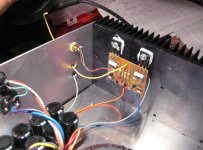
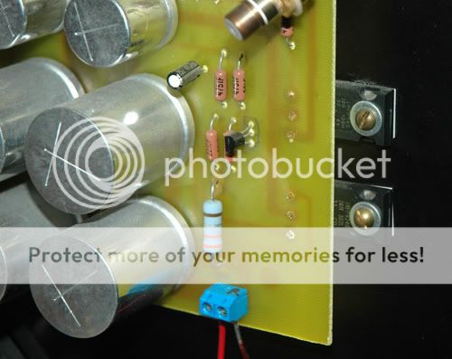
Yowza, watch them pots to adjust bias - definitely start with them at zero as midway juicing 1.8 volt on 0.47 (3+ amps) bringin smoke, ehhe - gotta love how tough these mosfets are.
DC offset adjustment seemed painless.
Better get back and check bias... left out the thermasistor since didn't have on hand.
Can I insert a R0 between 100k ground/signal ground and the 2 - 10 ohm resitors to ground? Connecting the the ground point for those 2 -10ohm to power supply ground. I'm getting faint ground loop noise and using traditional technique for creating pure ground at center of power cap bank...
Attachments
Variac said:Can you make a power supply with just chokes and resistors and no caps? That would be thematically correct!
wakoo Mod !
ya have Niagara in backyard ?

spencer said:Assume supply is +/- 24v, current through R5, R1, R2, R6 will be :
48v / 2.2k = 2.2 mA max, assume J1 and J2 is not there.
I am afraid that 48V/2.2k = 22mA
traw said:
Yowza, watch them pots to adjust bias - definitely start with them at zero as midway juicing 1.8 volt on 0.47 (3+ amps) bringin smoke, ehhe - gotta love how tough these mosfets are.
I was gonna say the same thing -- and this just from the simulation. I set the pots to 1% per click and just a small change can really affect the bias. NP makes this point quite clearly in the AX article (it arrived yesterday afternoon) so everyone is recommended to start at 0.
I had a couple of prototype boards burned (don't have the time right now to make my own.) If I were to do it again I would put the output MOSFETs further apart since this thing really cooks. A 0.6 C/W heat sink is recommended.
Notice article suggest fairly good size of heatsinking to satisfy the c/w details. I used borderline as myself running without the therm comp thus probably not good idea, for my situation, to run it like an aleph (sizzlin).
Only listened to for about an hour late last night. Ran warm-hot but not too bad. Will check steady state over weekend.
Nice immediate and natural sound. Can tell it's as stated in article, lowest distortion one yet. Gain feels higher than 15db, or seems good bit louder than my F3 (13.5db).
Only listened to for about an hour late last night. Ran warm-hot but not too bad. Will check steady state over weekend.
Nice immediate and natural sound. Can tell it's as stated in article, lowest distortion one yet. Gain feels higher than 15db, or seems good bit louder than my F3 (13.5db).
Variac said:
Can you make a power supply with just chokes and resistors and no caps?
In theory, yes. In practice it's difficult because you need some form of energy storage and getting (even winding your own) big enough coils would be difficult and expensive. And heavy. And bulky.
The storage in an inductor is in the magnetic flux surrounding the coil. The bigger the coil, the more flux. It's when the flux lines collapse that the current flows (which is why you see diodes across relay coils--keeps the backlash from roasting parts), but it tends towards sharp spikes so you need an inductor to smooth the spike from the inductor to smooth the spike from the inductor to smooth the spike from the inductor...
Grey
Variac said:Can you make a power supply with just chokes and resistors and no caps? That would be thematically correct!
Inductors would be ideal for amplifiers that want a forced constant
current draw instead of voltage. Just as conventional amplifiers want
a constant supply voltage but draw current variably, this amplifier
would want constant current and would create a variable voltage
at the supply input.
Here's a conceptual PCB design which will probably do a better job of diffusing the heat -- the MOSFET's are on the wings (and are mounted with pins coming from underneath the PCB). The PCB is 3.7" * 1.8".
An externally hosted image should be here but it was not working when we last tested it.
jackinnj said:Here's a conceptual PCB design which will probably do a better job of diffusing the heat -- the MOSFET's are on the wings (and are mounted with pins coming from underneath the PCB). The PCB is 3.7" * 1.8".
An externally hosted image should be here but it was not working when we last tested it.
Conceptually looks great really, you got my humble blessing.

I would put those power resistos flat over the board though, even if that means a bigger PCB
> Here's a conceptual PCB design
IMHO :
1) I would use a foil resistor at the MOSFET source (R11), like e.g. MPC74 0R47, which has a similar footprint as wire wound ceramic resistors.
2) I would place TH1 directly on the MOSFETs for thermal compensation.
3) I would place R13 as close to the MOSFET gate as possible.
4) I would place R3, P1, R15 as close to R13 & R11 as possible.
5) R19, R17, R21 and the BJT can be placed further away, as they are only for protection.
In addition, the feedback path also want to be as short as possible, without saying.
Patrick
The thought I had was to do with trying to get the heatsink disapating the energy quickly and evenly as soon as possible. So rather than having one central hot spot space them out to use more of the heatsink surface. I am not sure if it is an issue or not, I guess that would depend on the heatsink.
SCD said:
... I guess that would depend on the heatsink.
In the end thats the point.
If space allow I would spread the power transistors... but hen again my Aleph4 runs them at 1 1/8" pitch, there are 12 FET's per channel on this one and no problems.
BTW, EUVL points are to be considered on the detail design, no doubt about that
> I guess that would depend on the heatsink
To be more precise, it is about your thermal management strategy.
Apart from wanting a short electrical path with low resistance and inductance between power FETs (i.e. assuming you get that one solved one way or another), you DO want to have all FETs thermally well coupled so that they have the same temperature at all times as much as possible, so that they drift together in the same manner.
On the other hand, you might NOT want all 200W or whatever that you are going to burn to be all concentrated at a 50x50mm patch if your heatsink is say 400x200mm, because you are then likely to get uneven temperature distribution on the heatsink and therefore not making the most effective use of that.
How you balance one against the other is art. And everyone has his own preferences.
Patrick
- Home
- Amplifiers
- Pass Labs
- F5 power amplifier