> In search for the x-ed f5 .... ?
http://www.diyaudio.com/forums/showthread.php?postid=1485083#post1485083
"The only remaning question for me is :
If I wish to go balanced, should I just use two of these or should I use complementary diff pairs for the first stage and Xed feedback ?"
http://www.diyaudio.com/forums/showthread.php?postid=1485298#post1485298
"4) The question of using dual diff pairs is moot, as you will need 2 pair of JFETs in either case. The effort required to run the feedback back to the Gates versus the Sources is not much, so you can explore this without much effort."
http://www.diyaudio.com/forums/showthread.php?postid=1486951#post1486951
"anyway - I can't see easy X-ing that circuit , without resorting to good ole "out to gate " feedback scheme , and that way we are loosing virtues of low impedance feedback path ......... "
All the answers were there, IMHO !!
> I would spread them out more if I could.
If you could somehow spread the heat out without moving the transistors furhter apart, would you still wish to do so ?
Patrick
Spread them
I think you could use tenticles on the pins of the mosfets if you want to get max spread or optimum positioning on the heatsink. This would mean the board would have to be separately mounted.
I do like to be able to use the pins to "hold" the board. Therefore,perhaps a bit longer board may be a useable option.
EUVL said:> I guess that would depend on the heatsink
To be more precise, it is about your thermal management strategy.
Apart from wanting a short electrical path with low resistance and inductance between power FETs (i.e. assuming you get that one solved one way or another), you DO want to have all FETs thermally well coupled so that they have the same temperature at all times as much as possible, so that they drift together in the same manner.
On the other hand, you might NOT want all 200W or whatever that you are going to burn to be all concentrated at a 50x50mm patch if your heatsink is say 400x200mm, because you are then likely to get uneven temperature distribution on the heatsink and therefore not making the most effective use of that.
How you balance one against the other is art. And everyone has his own preferences.
Patrick
EUVL is exactly right. I might add though,,, that the heat sink needs to have the flat mounting surface very thick in order to avoid the temp difference problem. Or, put another way, Heat wants to spread out and radiate like the disspersion of a speaker. When you put a restrictive tunnel like path for the speaker to radiate into (a Horn) you create a resistance to the diaphram. In open air it see's much less resistance. If the heatsink has a thin mounting surface, the heat sees a resistance to spreading across the surface. A thick mounting surface improves the ability to spread laterally across the mounting surface (efficiency). 3/8" or better is good if you want to spread the devices apart several inches. Sorry about the inches, I gave the day job way to much of my brain power this week

moe29 said:
does FET spacing really matter? I'm sure more space can't hurt, but is it something to fret about?
I dropped in on a heatsink thread last week, only to find that others had different impressions of how to manage heat. At the risk of ruffling even more feathers, I'll go so far as to say that for an average heatsink, I'd mount the devices in a horizontal row about 1/4 to 1/3 of the way up from the bottom. Take the horizontal dimension and divide it by the number of devices so that you've got something like, for example, 3 horizontal inches per device, then space them accordingly. The first device across will be mounted 1/2 of its assigned width from the edge (i.e. 1.5"). The next one will be mounted the full 3" away, etc., until you get to the last one which will again be 1/2 of its distance from the edge.
You can get fancier than that, of course, and sometimes other factors come into play, like structural members, but it's a pretty good rule of thumb system. The basic idea is to spread the heat out, not concentrate it all in one place. Yes, the laws of thermodynamics dictate that heat energy goes from places where there is more of it to places where there is less of it, but there's no reason to make it 160 degrees fading to 100 degrees at the edge when you can make it 130 degrees fading to 100. Be kind to your devices and they will be kind to you.
If you find yourself faced with a really tall heatsink and it's going to stay that way for one reason or another, try to put some of your devices in a second horizontal line roughly half-way between the bottom row and the top. It's not perfect, but it'll get you through.
Yes, there are simulation programs for this sort of thing, but I'd suggest taking the results with a grain of salt.
If you use fans, everything changes.
If you go with water cooling, you can get away with just about anything you care to try. Take it from someone who runs TO-220 devices at 30W each and has never had a device fail. Yet. (Now, I've gone and angered the audio gods. I will regret saying that.)
Grey
cicuitry testing / designing
Small question, what software is it you use to draw / test circuitry ?
regards
jackinnj said:Every afternoon I sit by the mailbox awaiting the current issue of AudioXpress...
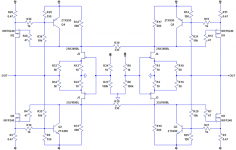
Just a quick sim -- this one tweaking the pots for minimum DC offset:
An externally hosted image should be here but it was not working when we last tested it.
Small question, what software is it you use to draw / test circuitry ?
regards
GOT My copy today!!!!Luckily I have The MINI-A project under weigh ...gives me time to wait out the PCB Group Buy to gather sTeam.
But you know somethin' ?...Looks like a P2P setup could really do it! NO CAPS!!!
And what's more...I GOT ALL THE PARTS.
Time to do some PLUMBING.
Thanks Nelson Pass.
But you know somethin' ?...Looks like a P2P setup could really do it! NO CAPS!!!
And what's more...I GOT ALL THE PARTS.
Time to do some PLUMBING.
Thanks Nelson Pass.
Re: cicuitry testing / designing
Yes, it's MultiSim -- all the ill-gotten gains of the Tech-DIY webstore go to pay for my licenses (and Bordeaux). You can get a version with some good functionality, but a limited number of nodes on the Analog Devices website.
jack
Nicola said:
Small question, what software is it you use to draw / test circuitry ?
regards
Yes, it's MultiSim -- all the ill-gotten gains of the Tech-DIY webstore go to pay for my licenses (and Bordeaux). You can get a version with some good functionality, but a limited number of nodes on the Analog Devices website.
jack
apassgear said:
Conceptually looks great really, you got my humble blessing.
I would put those power resistos flat over the board though, even if that means a bigger PCB

They get the heat away from the board quite effectively -- but they also require a pin-header to measure the bias current.
lumanauw said:Around the output stage limiter, what is the function of 10K (connected to output node)?
Hi Lumanauw,
Oh . . . you are a member of the
 mafia . . .
Understanding the designer's intention fully, just by looking the
circuit, is always difficult. I just presume that the 10K watches the
output voltage and limit the voltage increase (or decrease) to the
certain level so that the minimum necessary Vds of the acting
gain MOSFET can be maintained.
a) Thermal simulation software are quite accurate. I have managed to get to within 2degC on a 40degC temperature rise between measured and calculated.
b) If you can find some published pictures of the XA160 or XA200 inside, you will see that Nelson did not mount the devices directly onto the (black) heatsink, but on thick aluminium heat spreaders which span over the entire heatsink surface. You are then no longer limited by the thickness of the heatsink base plate itself. I have give you enough hints.
Patrick
EUVL said:> Here's a conceptual PCB design
IMHO :
1) I would use a foil resistor at the MOSFET source (R11), like e.g. MPC74 0R47, which has a similar footprint as wire wound ceramic resistors.
2) I would place TH1 directly on the MOSFETs for thermal compensation.
3) I would place R13 as close to the MOSFET gate as possible.
4) I would place R3, P1, R15 as close to R13 & R11 as possible.
5) R19, R17, R21 and the BJT can be placed further away, as they are only for protection.
In addition, the feedback path also want to be as short as possible, without saying.
Patrick
1) I'll try it with both a metal foil ceramic and WW --
2) The thermistor can be mounted on the device or on the HS.
3) R13/14 are a few mm from the gates
4) As R11 heats, the resistance of R3 and P1 (etc.) will increase -- wouldn't you want R3/P1 R4/P2 further away from R11/12?
What would you suggest as a temperature coefficient for the thermistor?
When I get the boards wired up I will run them on my spec analyzer out to a few MHz -- as the gate stoppers are purposefully low...
For myself, I almost always use TO220 or TO247 (e.g. Caddock) power resistors for source degeneration. Which means I just mount them on the heatsink next to the FETs, and hard wire from source to resistor. As such, components on the PCB do not see any of the major heat dissipating elements directly.
But then some of you might want something less expensive. So that was why I gave you another tipp to use MPC71 or MPC74 :
http://www.nova-elektronik.de/english/resistors/mpc.php
http://www.buerklin.com/
If you mount them on the PCB, such that the ceramic body is say 4mm above PCB (either with a knick in the leads, or a ceramic standoff), 1/4W resistors lying flat on the PCB will also see very little of that heat. In a Class A amp, everything sees the heatsink temperature (say 55 degC) eventually. So I would say your worry is undue.
Tempco of the NTC depends on the tempco of the FETs, which is different from FET to FET. For IR FETs, you'll have to ask Nelson.
For R1 & R2, you can always parallel 2x or 3x 2W resistors to reduce the tolerance and inductance.
Patrick
Onvinyl said:Does the F5 need to see an easy load to work best or might I treat it with a complex passive Loudspeaker X-over?
Stabilitywise those drain outputs should work great.
Rüdiger
naah - just shoot him with everything you have

- Home
- Amplifiers
- Pass Labs
- F5 power amplifier