Patrick,
Really ?
It has been my experience that higher i/p stage current requires smaller values of i/p stage o/p resitors for a given o/p stage bias current, and this gives less OLG & less FB.
Would not increasing the value of R1&2 decrease the OLG & FB even further ?
If we feel the need to adjust for this lost FB I think the resistors R&2 and 5-8 need to be decreased in value
But I really don't think it is necessary to bother to adjust these resistors - there is plently of FB so a little less will be just fine
Last edited:
The open loop gain of the input stage is given by Rdrain / ( Rsource + 1/Yfs ).
In this case 1/Yfs is the dominant contributor (about 30R).
Increasing Rsource reduces the JFET bias, which in turn means a higher Rdrain to give the same bias voltage for the output stage.
So the net result is an increase in OLG by ~2dB, according to LT Spice.
But I also would not bother with difference in 2dB loop gain.
Cheers,
Patrick
Thanks for the feedback, guys. 
I was wondering what effect the lower value JFETs had on the overall sound, and that helps clear things up for me. But it does make me wonder why JFETs in the 9-11mA range go for more money than those with a lower range. It seems like it should be the other way around.
I was wondering what effect the lower value JFETs had on the overall sound, and that helps clear things up for me. But it does make me wonder why JFETs in the 9-11mA range go for more money than those with a lower range. It seems like it should be the other way around.
Hello ladies and gents,
Finally i got my F5 quiet and running like it should - YEYY....
...
Had the oportunity to take few shots of the amplifier with thermography camera - thought you might be interested to see....
Amplifier PCB is from diyaudio store and psu as well....
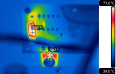
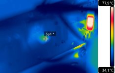
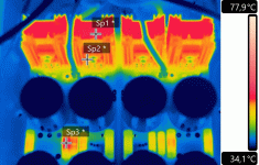
First picture is power supply board.
Second picture is one side of the amplifier board with 0R47 and one of the output mosfets
Third picture is input pair in the middle.....
Finally i got my F5 quiet and running like it should - YEYY....
...
Had the oportunity to take few shots of the amplifier with thermography camera - thought you might be interested to see....
Amplifier PCB is from diyaudio store and psu as well....
- power supply diodes are FEP30 with heatsinks - diodes are running at 52 Celsius
- resistors in output pair (0.47R) are 5W running at 83 degrees Celsius
- Big heatsink is at 43 degrees
- input pair (jfet) are at 53 degrees
- output pair are at 78 degrees (IS THIS SAFE ENOUGH - long term?)
First picture is power supply board.
Second picture is one side of the amplifier board with 0R47 and one of the output mosfets
Third picture is input pair in the middle.....
Attachments
78 to 43 is a pretty big delta - how long was the amplifier running for when you took the picture?
I see no more than 15C with ordinary measures, and better than 10C when using thinned mica, good computer grease and a copper heatspreader.
78C Tcase = ~108C die temp, this is not unsafe, but better to aim lower.
I see no more than 15C with ordinary measures, and better than 10C when using thinned mica, good computer grease and a copper heatspreader.
78C Tcase = ~108C die temp, this is not unsafe, but better to aim lower.
i agree on that - i was specifically trying to see what to use best not to get into this problem and from what i understand is that ceramic pads are the best to use... from what i saw, 3mm or thinner was not to much of a difference... should be fine either way....
that is why i used these....
what bothers me is that i can hold my finger on those transistors for as long as you want me to hold it...
under the nut the temperature is not that big - it is closer to 58 degrees - only where the chip is inside, you can see that temperature... so maybe the gousing is thin there and it shows the temperature of the chip actually on the case of the mosfet... which would be reasonable to say i think.... the temperature of the metal part of the transistor is lower for sure i think..
seems to me that i am right here (upon checking those pictures again)....
what i read on the side of the transistor case where the screw is is a case temperature which is 58
what i read at the bottom of the case of the transistor where the legs are is actually the temperature of the chip inside transfered through the plastic of the case... that sounds about right also because i can hold my finger as long as you want on the screw side of the transistor.... can't get towards that part where the chip is inside because of the ntc that is ower there....
so, i think that the chip would not be on 78 degrees but lets say on 90 degrees or so inside...
which should be o.k. imho.....
correct me if i am wrong....
3mm insulators must never be used for a class a design like this. At least not if run fully biased. My reference is Zen Mod. Though Sangram is probably saying just the same, but more politely than my Viking directness.
Kheratherm is perfect and just as unmessy as pads.
But, changing now will mean desoldering the mosfets and is perhaps not worth it if the amp runs fine.
@ 78 degrees, if correct, the die will perhaps run too hot in the long term, if I remember correctly. Forgot the math for that, and don’t have time to check. Anyways, amps using thick silicone pads have broken down and been debugged in this forum before. Just a fair warning. You need to get more of the heat out of the mosfets and into the sink. Those pads hinder that.
That said, I am NOT an expert. This is just my opinion, based on what other have said before and some math I did myself a good while back. Note also that the Kheratherms are a bit fragile. You need to ensure the mosfets are fastened evenely to the sink and also torqued before any soldering is done. Otherwise you risk breaking them and making contact between fet and sink.
i am not using thick silicone pads but ceramic pads...
.
on internet the claim that ceramic pads can handle 20-28W/mK and Keratherm 2.5-3.5W/mK.... what i understand, ceramic looks way better....
.
also, as said - seems to me that the case of the transistor is lower in temperature and that what i see here is actually the part where chip is transmitting through the plastic - explained it above better (not to repeat)
.
on internet the claim that ceramic pads can handle 20-28W/mK and Keratherm 2.5-3.5W/mK.... what i understand, ceramic looks way better....
.
also, as said - seems to me that the case of the transistor is lower in temperature and that what i see here is actually the part where chip is transmitting through the plastic - explained it above better (not to repeat
)
Last edited:
I have a question....
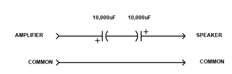
I have F5 running.... it is a hot amplifier and i don't have a speaker protection circuit at the output and there is very little room in the box.... would it be maybe safer to put a 4700uf capacitor at the output of the amplifier... just in case something goes wrong.....??
I have F5 running.... it is a hot amplifier and i don't have a speaker protection circuit at the output and there is very little room in the box.... would it be maybe safer to put a 4700uf capacitor at the output of the amplifier... just in case something goes wrong.....??
Have completed a stock v3 F5 build. Plays rather nice, but has a tiny bit of audible hum if I put my ear right next to the speaker. Does not go away if I short the inputs on the board. I have 88000 uF on each rail, giving about 60mV ripple with about 1A bias. I tried with a 3rd filter bank as well with an additional 27000uF pr channel and rail. This brought down the ripple to around 20mV but made no difference on the hum, if anything it got a bit worse.
The big surprise came when trying to look for the hum with the scope on the outputs. There I find a significant amount of RF noise in the Long wave band, 150 to 350 kHz. Anyone seen something similar or any clue to where to start looking for that problem? Will try tomorrow to trace backwards to see if I can spot where this first occurs in the chain / amp. RF noise decreased when shorting the inputs , but did not completely disappear.
The big surprise came when trying to look for the hum with the scope on the outputs. There I find a significant amount of RF noise in the Long wave band, 150 to 350 kHz. Anyone seen something similar or any clue to where to start looking for that problem? Will try tomorrow to trace backwards to see if I can spot where this first occurs in the chain / amp. RF noise decreased when shorting the inputs , but did not completely disappear.
I have F5 running.would it be maybe safer to put a 4700uf capacitor at the output of the amplifier.
That's possible, but it must be bipolar (two identical capacitors in an "anti-series" connection.
Attachments
IvarNy, I do not have any experience with RF noise but noise in the audible band can be due to other factors besides power supply ripple. Layout of components and wring arrangement can have a major effect on electromagnetic interference and noise pickup.
Pictures of the interior of your amplifier may provide some insight into your hum issue.
Pictures of the interior of your amplifier may provide some insight into your hum issue.
There has just been a similar issue with hum and it got solved. Maybe good to check the solution to the hum issue?
I think it was "sparkle" which had the issue and got it solved by almost rebuilding the amp and change the wiring?
Maybe "sparkle" can give a quick "wrap up" of what solved it or "IvarNy" can check back in this thread what caused the hum?
I think it was "sparkle" which had the issue and got it solved by almost rebuilding the amp and change the wiring?
Maybe "sparkle" can give a quick "wrap up" of what solved it or "IvarNy" can check back in this thread what caused the hum?
I Found that the RF noise came from the DAC I was using to generate test tones etc. So that mystery was solved. Tested swapping out the F5 cards with F4 cards and those are dead silent, so I'll run with those for while and probably build an new and bigger chassis for the F5, as it was a little crowded. I am suspecting it was silent when on the bench with the heat sinks laid on side, but when assembled, the humm appear. Probably some components close to inputs are too close to the torroid, may install some iron casing around the torroid in the next build.
- Home
- Amplifiers
- Pass Labs
- F5 power amplifier