I could draw it, but that won't help you, since I can't show you any of my drawings.
Do you have a cameraphone?
See attached close-up. I can't remove the boards at the moment to take a photo of the under-side.
I can't find any info on the KR4002. Thought it might be equivalent in the same way that a LSK170 ~= 2SK170. Same part, different manufacturer. I'll get some 1N4002s to be safe.
I can't find any info on the KR4002. Thought it might be equivalent in the same way that a LSK170 ~= 2SK170. Same part, different manufacturer. I'll get some 1N4002s to be safe.
Attachments
the signal return/ground has to go somewhere when it enters the PCB.
Where does it go?
That was what I could not see in the first pic, nor in the second pic.
Remember what I keep having to repeat. The input CIRCUIT must remain as a circuit and (preferably) all the Flow and Return traces should be close coupled.
Where does it go?
That was what I could not see in the first pic, nor in the second pic.
Remember what I keep having to repeat. The input CIRCUIT must remain as a circuit and (preferably) all the Flow and Return traces should be close coupled.
I buy 1n4002 or 1n4004 by the hundred.I can't find any info on the KR4002. Thought it might be equivalent in the same way that a LSK170 ~= 2SK170. Same part, different manufacturer. I'll get some 1N4002s to be safe.
Many give a good discount at this number.
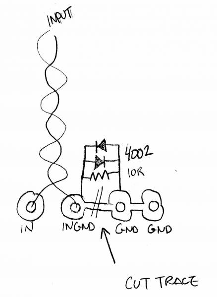
OK, I see the problem. Cutting the trace and adding the HBR there would put the HBR in the signal path. But I don't see any other path for input gnd other than through the common power ground as seen on the board. I don't think there are any traces on the under-side of the board connecting the input ground to anything else (would appear as dark lines on the attached photo (without my yellow arrow obstructing the view)).
So, to implement Joffe, I might have to not only cut the trace and add the HBR, but also add a jumper (to where?) to complete the input signal circuit.
Again, this is well beyond my level of understanding, so correct me if I'm wrong in any of my assumptions or conclusions.
So, to implement Joffe, I might have to not only cut the trace and add the HBR, but also add a jumper (to where?) to complete the input signal circuit.
Again, this is well beyond my level of understanding, so correct me if I'm wrong in any of my assumptions or conclusions.
Attachments

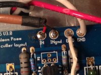
Not sure I can see the detail, but here goes.
The pads at the centre top are left to right
IN, INgnd, GND, GND
IN connects down to a wide left to right trace. This wide trace has two components at it's ends, are they resistors?
INgnd connects right to GND
left GND has two connections, down to a pad and down again to a capacitor
and right to the right GND
right GND connects via a thin trace to a LED pad and maybe a diode?
Back to the left GND.
This looks like part of the INput circuit.
What are the components just below the left GND?
What traces are on the bottom side of the PCB. The right GND cannot just stop there. It must go somewhere.
Andrew, thanks again for taking the time to help figure this out. Sorry I didn't reply earlier but it's been a busy week.
Anyway, here's what I can offer:
At this point the hum is barely audible unless you put your ear right up to the speaker, so I'm going to take a hiatus from tackling this issue for a while (playing around with JBOZ and ACA now") ). My son is enjoying the F5 immensely, and I'll just let him keep enjoying it for a while. But, if you think there's a way to implement Joffe, given the board layout, I'm open to suggestions. At some point I'll also look into making a simple EMF shield for the transformers.
). My son is enjoying the F5 immensely, and I'll just let him keep enjoying it for a while. But, if you think there's a way to implement Joffe, given the board layout, I'm open to suggestions. At some point I'll also look into making a simple EMF shield for the transformers.
My son took some money my dad gave him and bought a used scope. He's figuring out how to use it so we'll measure the hum and post any useful info.
Speaking of the scope, time to post something in the JBOZ thread...
Anyway, here's what I can offer:
Yes, R1 & R2 on the V.3 schem. 4.75R & 47.5K respectivelyNot sure I can see the detail, but here goes.
The pads at the centre top are left to right
IN, INgnd, GND, GND
IN connects down to a wide left to right trace. This wide trace has two components at it's ends, are they resistors?
No, the 4 pads aligned below the left GND are for R3 (extra holes for alternative resistor case styles, I guess). No capacitor (this is an F5, after all).INgnd connects right to GND
left GND has two connections, down to a pad and down again to a capacitor
Yes. Don't know what the diode's for... optional, not in the schem.and right to the right GND
right GND connects via a thin trace to a LED pad and maybe a diode?
R2 and R3.Back to the left GND.
This looks like part of the INput circuit.
What are the components just below the left GND?
I can't take the boards out at the moment to see the bottom traces. The darker lines on the photo of the board (from the diyAudio store page) show the bottom-side traces (at least those portions not obscured by the top-side traces). I can tell from the photo (linked below, again) that InGND, LeftGND, and RightGND are interconnected, and also connect to R1, R2, R3, R4, and the wiper pin on P3 (not used in my build). This is consistent with the schem, and thus I don't think there are any additional traces connected to GND on the bottom side of the board.What traces are on the bottom side of the PCB. The right GND cannot just stop there. It must go somewhere.
At this point the hum is barely audible unless you put your ear right up to the speaker, so I'm going to take a hiatus from tackling this issue for a while (playing around with JBOZ and ACA now
). My son is enjoying the F5 immensely, and I'll just let him keep enjoying it for a while. But, if you think there's a way to implement Joffe, given the board layout, I'm open to suggestions. At some point I'll also look into making a simple EMF shield for the transformers.My son took some money my dad gave him and bought a used scope. He's figuring out how to use it so we'll measure the hum and post any useful info.
Speaking of the scope, time to post something in the JBOZ thread...
Attachments
Is there any chance to boost the amplification of the f5 ?
I've finished mine, and its directly connected to the CD-Player, but it seems that the CD-Player doesn't have enough level to drive the Amp.
I don't want to have any Preamp between source and amp.
Thanks again for your friendly support
I've finished mine, and its directly connected to the CD-Player, but it seems that the CD-Player doesn't have enough level to drive the Amp.
I don't want to have any Preamp between source and amp.
Thanks again for your friendly support
This "gain" question has been answered many times.
Even Pass talks about it in the pdfs that he has published.
A standard F5 has a gain of 6times (~+15.6dB)
The standard F5 has a maximum output of ~20Vp, equivalent to ~14.1vac
The standard F5 has an input sensitvity of ~2.35Vac for maximum power.
If your CDP has a maximum output around the normal 2Vac to 2.2Vac, then it cannot drive the standard F5 into clipping.
But it can get pretty damned close !
Why can't you give us some information so that we can help?which iteration exactly you're using (sch , pcb ) ?
which iteration exactly you're using (sch , pcb ) ?
I'm using the pcb from diy-audio-shop, have a look at http://anleitung.diy-audio-shop.de/F5.pdf
This "gain" question has been answered many times.
I'm really sorry, I know that there is lots of information in this thread, but I haven't read all of the 1466 pages of threads yet. I'm new to this amp so I might have some problems that somebody else had too.
That you Andrew for packing all information together.
Is there any chance to change the gain?
Is there any chance to change the gain?
Yes, less feedback = more closed loop gain. Do a search for feedback and you will see lots of discussion. Trade off is higher distortion.
Rush
This thread may help.
http://www.diyaudio.com/forums/pass-labs/240822-how-hot-can-i-bias-my-f5.html
Also some of us have changed R5-8 to 220R resistors.
http://www.diyaudio.com/forums/pass-labs/240822-how-hot-can-i-bias-my-f5.html
Also some of us have changed R5-8 to 220R resistors.
............I don't want to have any Preamp between source and amp.........
Where is the volume control in your system? Integrated in the CDP?
Since there is a "device" between the CDP and Amp let me suggest the O2 unit to replace the pot. I bought the rather inexpensive kit version and it is super quiet/clean and accurate. Was exactly what I needed for both the F5 and BA-3 as I needed just a bit more SPL with the speakers I'm using. That's not what you proposed, but might be worth your consideration.
- Home
- Amplifiers
- Pass Labs
- F5 power amplifier