It takes practice. I can finish those 4 boards completely with all components (including through hole) in less than an hour.
Your solder is probably too large in diameter, so you end up with too much solder on each pad.
(As said before, suggest you use 0.35mm solder. I find 0.5mm already too thick.)
This is still not a problem, as you can (even now) remove excess solder with a fine solder wick (0.8mm or 1mm).
Even though your current soldering is electrically OK, I still suggest you try to remove the excess solder.
This is especially true for active devices with gull wing leads.
The gull wings leads are there to provide elasticity to accommodate differential thermal expansion.
(Your soldering and working temperatures are likely to be different).
The excess solder will take away this elasticity, which results in excessive stress at the leads, especially at the edge of the epoxy moulded case.
In the long term, this will become a reliability issue.
So before you do anything else with your current PCBs, suggest you get some cheap 0805 resistors locally.
Practice component positioning, soldering and solder removal on a strip board.
Once you get the hang of it, then try to remove excessive solder on your current boards.
At least for the BJTs and the diodes.
The regulator boards are cut from a large panelised board.
You need to use a small file or a sanding block with #120 wet & dry sand paper to touch up the corners.
Only cosmetics, I know. See the photos from cloud85.
Patrick
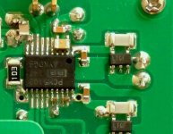
Here is an example from year 2012, our PCM5102 DAC board.
The smallest component here is of 0402 size, half the size of the 0805 you are using.
You cannot hold them properly with bad tweezers.
Note how little solder.
Today, I would even use less solder than in this example.
The most important is the solder between the leg and the PCB, and not around or on top of it.
Practice makes thing perfect.
Patrick
Attachments
Let's watch some video :
https://www.youtube.com/watch?v=66GV4OuShzI
Another approach (which I find too messy) :
https://www.youtube.com/watch?v=PtcdCGA_qTk
Patrick
https://www.youtube.com/watch?v=66GV4OuShzI
Another approach (which I find too messy) :
https://www.youtube.com/watch?v=PtcdCGA_qTk
Patrick
Last edited:
Thanks Patrick for the info and resources, the solder I used is 0.38mm Eutectic ones, I put too much in the novice thought that it's "safer"
Time to get some fine solder wick from the local electronic store, good learning experience")
Get a good solder wick, some solder wick are more trouble than help. I like the Goot band
Nice Patrick!
I learned to do SMT soldering 20 years ago working in a AT&T, and later on Lucent manufacturing plant. It's like riding a bike, it is never forgotten...
After 20 years of not touching a soldering iron, kids and so on... you know... I produced this last year, using 0.5 mm solder and my +3 glasses
Less is more indeed, and very quick, short pulsed soldering is the best
I learned to do SMT soldering 20 years ago working in a AT&T, and later on Lucent manufacturing plant. It's like riding a bike, it is never forgotten...
After 20 years of not touching a soldering iron, kids and so on...
you know... I produced this last year, using 0.5 mm solder and my +3 glasses Less is more indeed, and very quick, short pulsed soldering is the best
Attachments
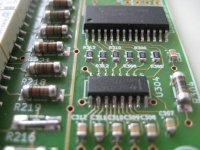
... At least for the BJTs and the diodes. ...
I think I'll settle with this, still novice quality but at least the gull wings are now exposed.
I'm starting to find myself more comfortable with these SMD babies, thanks to this F5-HA project
Attachments
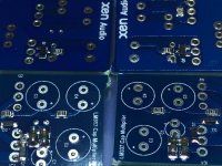
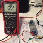
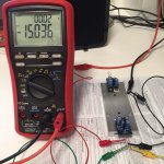
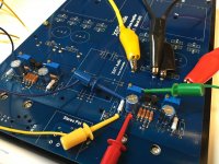
The 4 CM boards are done, a quick test showed they're giving the expected voltages.
Both positive reg are giving around 15.2V, and both negative reg around are giving -15.0V. If they're big fat through hole boards I will replace some resisters to give same value on both sides, but not with these compact boards
Both positive reg are giving around 15.2V, and both negative reg around are giving -15.0V. If they're big fat through hole boards I will replace some resisters to give same value on both sides, but not with these compact boards
Attachments
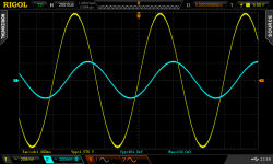
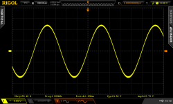
I soldered the CMoy Linkwitz cross feed module today, and tested it. If I feed 1 kHz sine wave into one channel only, there are attenuated output at both channels, so I think it's working though I'm not entirely sure.
I have two other questions:
I have two other questions:
- J1 (Perspective Jumper) - what is this for?
- With a square wave input at one channel, the cross feed output at the other channel is clearly bandwidth limited. However, I do find some nice square wave response at Fig. 7 of the official build guide. Are those response obtained when the cross feed is disabled? (and this is why I'm not sure if the cross feed module I built are working properly)
Attachments
> J1 (Perspective Jumper) - what is this for?
This is according to CMoy.
It reduces cross feed and therefore widens the sound stage.
If you are using Danyuk then just leave open.
> However, I do find some nice square wave response at Fig. 7 of the official build guide. > Are those response obtained when the cross feed is disabled?
Correct.
Patrick
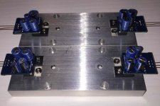
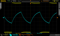
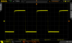
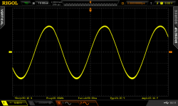
A bit more soldering today, bias to 150mA, and tested the 2 channels with a bench power supply.
There is a slight undershoot at the bottom of the 20kHz square wave output, so I may need to increase the output gate stopper.
Also, the lines seem to be a bit "thick" but I believe it's due to my noisy switchmode power supply, hopefully they'll look better once I switch to a normal linear power supply, otherwise will need to look for oscillations.
Attachments

I would not change the gate stoppers. It is just cosmetics.
Use a linear PSU and perhaps add some load to see if you still have those "thick" traces.
In all the versions we have built, we have not had stability issues.
But then we also have not tried 2SK2013 / 2SK313.
(Not that they should make any difference.)
But you are 90% there already.
Patrick
Use a linear PSU and perhaps add some load to see if you still have those "thick" traces.
In all the versions we have built, we have not had stability issues.
But then we also have not tried 2SK2013 / 2SK313.
(Not that they should make any difference.)
But you are 90% there already.
Patrick
Thanks Patrick, so I'll just keep the gate stopper and save the trouble of desoldering.
I think I'm 90% done with the electronic parts (don't expect surprises with the transformer and diodes), but the most difficult part for me is yet to come - chassis, drilling and tapping, which I'm not too good at.
One request, I'm wondering if it's possible to email me the .drl drill file of the main board (just the .drl will do, no need for the rest of the Gerbers), reason being that I forgot to mark the drilling positions on the base plate before populating the PCB, and it's now quite difficult to do so. (In fact, I already ruined the base plate, fortunately the TB seller happens to have an extra one and willing to sell me that at low cost, so the cost is limited). With the .drl file, I can then print it out in scale and then do the marking.
Thanks and regards.
Are you using cross feed ?
If so I suggest you use a gain of 11 instead of 6.
I post here a DWG file for the bottom plate with all the holes required for mounting MOSFETs and PCB.
There are many free DWG reader software available, e.g. Draft Sight.
Just use any of them and print 1:1 in mm.
The plate outside dimensions are 246mm x 177mm on the drawing.
So you can use that to check your printer setting.
Patrick
Attachments
- Status
- This old topic is closed. If you want to reopen this topic, contact a moderator using the "Report Post" button.
- Home
- Amplifiers
- Pass Labs
- F5-HA Build Thread