I would hope you have 3.3 volts (or up to 5v) on pin21 of the tssop chip. That's VL or the logic voltage input. Depending on your design or the depth of your power supply mania, that could be attached to Vd or it's own supply.
The three main chips in this dac design (excluding the USB chip) have a total of seven voltage inputs. They are:
CS8416: Va, Vd, VL
CS8421: Vd, VL
CS4398: Vd, Va
The three main chips in this dac design (excluding the USB chip) have a total of seven voltage inputs. They are:
CS8416: Va, Vd, VL
CS8421: Vd, VL
CS4398: Vd, Va
Check pin1 on 8416 I have 5v there and no voltage (and no sound) with the first regulator dissconnected.
With 1 or 2 regs I have nothing at PIN1 but I do have sound.
On 4398 pin 17 wich is vref I have 11v.And it seems that the Vd is 3,3v to.
And the Va is +5v from the middle 5v reg.
The cs8421 has its local 3,3v reg,that is feed from a 5v supply,ill try to locate later this evening wich 5v it is.
And the Va is +5v from the middle 5v reg.
Do you think it would be an improvement to do this?As far as I have read digital supplys isn´t as sensetive as analog ones,or?That's VL or the logic voltage input. Depending on your design or the depth of your power supply mania, that could be attached to Vd or it's own supply.
The cs8421 has its local 3,3v reg,that is feed from a 5v supply,ill try to locate later this evening wich 5v it is.
With 1 or 2 regs I have nothing at PIN1 but I do have sound.
Pin1 on the CS8416 is the fourth input for spdif data. Since it's an input with nothing connected to it, it strikes me that it's likely to either float to ground or to the voltage rail. I don't have the gigawork schematic infrint of me at the moment, but I seem to recall that even with the USB option that the fourth input wasn't used.
Sheldon
Power transformer for DAC with output transformers?
Would there be any audible advantage to going with an R-Core transformer for just powering the DAC with 9v?
Not using opamps just Jensen transformer outputs.
Thanks!
Would there be any audible advantage to going with an R-Core transformer for just powering the DAC with 9v?
Not using opamps just Jensen transformer outputs.
Thanks!
Hi Michael,
I still suggest the upsampling version of the CS4398 board. The 8421 up sampling chip is much improved over previous generations, very smooth and articulate.
If you are going to try the opamp output circuit you will need a power trafo similar to the one offered by the seller with 12-0-12 and 8-9v windings. If you do away with the opamp circuit all you need is a single 7-12VAC trafo. The load is less than 250ma on the digital side so you don't need anything big.
I would hope you have 3.3 volts (or up to 5v) on pin21 of the tssop chip. That's VL or the logic voltage input. Depending on your design or the depth of your power supply mania, that could be attached to Vd or it's own supply.
The three main chips in this dac design (excluding the USB chip) have a total of seven voltage inputs. They are:
CS8416: Va, Vd, VL
CS8421: Vd, VL
CS4398: Vd, Va
Ok,this is it:
CS8416: Va, Vd, VL :All from the 3,3v small regulators.
CS8421: Vd, VL :From the 5v reg that´s between the middle 5v and the 13v reg,if you don´t have have an upsamplingboard,I dont know what this ones for?Messaure and check..
CS4398: Vd, Va :Va from the middle 5v reg. Vd from the 3,3v small regulators.
USB:Is the reg that I pointed out on my pictures.
Would there be any audible advantage to going with an R-Core transformer for just powering the DAC with 9v?
Not using opamps just Jensen transformer outputs.
Thanks!
If you think it will sound better with a particular type of trafo, it probably will. Some even suggest they can hear the difference between different brands. I don't buy it, but that's just my opinion.

Would anyone be able to explain where to connect 3.3V regs other than in the location where the original ones are. I'm supposing input could be taken at the "+" pin of each of the 1000uF lytics to the left(upstream) from the 1117s but I'm not sure where the ouput would go.Ok,this is it:
CS8416: Va, Vd, VL :All from the 3,3v small regulators.
This is the PSU section for the 5v and the 3,3v:
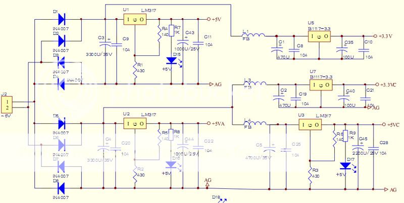
But the uF of the e-lyts do not match,so I think that the 1000Uf nearest the 3,3v reg should be the vinput you have to messaure that it is about 8v at that e-lyt.And the 1000uf some cm from the reg is the output,messaure.And it´s the same here,either remove the 3,3v reg or cut a track(output track).
Report back how its going..
Would anyone be able to explain where to connect 3.3V regs other than in the location where the original ones are. I'm supposing input could be taken at the "+" pin of each of the 1000uF lytics to the left(upstream) from the 1117s but I'm not sure where the ouput would go.
Do you want to know where on the chip they go?
On the CS8416 chip, pin6 is Va, pin23 is Vd, and pin21 is VL
The problem arises that the 8416 is on a daughter card in this unit, and I don't know if pin6 on the TSOP is pin6 on the DIP.
Sheldon
The problem is that the output pin from one of the old 1117s got damaged and is unusable. If I measure voltage with regs connected to + pins and ground(but not to output) I get about 5.6V. If I measure with reg output connected to + pins of the lytics to the right(upstream) of where 1117s used to be I get 3.3V but no sound. I get about 5.6V at 8416 pins 6, 21, 23. Obviously I'm not connecting output in the right place.
I just need to know how to bypass old reg location as I did with the 5V regs so that I can supply all 3.3V requirements - not just 8416
I just need to know how to bypass old reg location as I did with the 5V regs so that I can supply all 3.3V requirements - not just 8416
Would anyone be able to explain where to connect 3.3V regs other than in the location where the original ones are. I'm supposing input could be taken at the "+" pin of each of the 1000uF lytics to the left(upstream) from the 1117s but I'm not sure where the ouput would go.
I got the board, the caps to the left of the regs are the input side, looking from the edge of the board. The caps to the right are the output side. You can take the feed for the new regs right off the left cap, plus and ground. You can run the out to the right cap or the ferrite bead.
It does look like the 8416 is fed only from 3.3v.
The 4398 has both 5 and 3.3v.
The 8421 has a 5v feed, and also has it's own 3.3v reg for the XO, fed from the 5v feed.
The USB has a 5v feed with it's own 3.3v reg for its XO.
If you are going to supply them with one "new"3,3v reg,if you don´t choose to remove the old regs,you have to locate the output track from the 3,3v regs and cut them,and then connect them together so that both tracks get 3,3v from the "new" regulator.Maybee you should remove the 8416 and 4398 so you dont dammage them before you get it right.I just need to know how to bypass old reg location as I did with the 5V regs so that I can supply all 3.3V requirements - not just 8416
Edit:Bill Fuss was faster..
Old regs are gone.
I tried connecting + of cap to the left of 1117 location to the + of the cap immediately to the right with ground to the old 1117(location) ground pin. It didn't work.
If I connect output to ferrite beads am I not bypassing lytics that are to the right(downstream) of 1117 location?
Does this matter? And if I chose to connect to ferrite beads can any reg be connected to any ferrite?
Sorry for all these questions but I just want to understand before going ahead with this.
Last edited:
If you connect the new reg to the ferritebed you are before the original 3,3v reg.you should connect after them.You can do a resetive messaure from the + on the e-lyts that are after the original 3,3v reg to to either the 8416 and/or 8398, if you hit it right there should be 0 ohm.
If you connect the new reg to the ferritebed you are before the original 3,3v reg.you should connect after them.
I'm getting even more confused now.
The ferrite beads I'm referring to are between the far right lytic and the 4398. How can that be before the original regs?
If you connect the new reg to the ferritebed you are before the original 3,3v reg.you should connect after them.You can do a resetive messaure from the + on the e-lyts that are after the original 3,3v reg to to either the 8416 and/or 8398, if you hit it right there should be 0 ohm.
You obviously have a different board. Both my boards have ferrite beads after the regs.
Old regs are gone.
I tried connecting + of cap to the left of 1117 location to the + of the cap immediately to the right with ground to the old 1117(location) ground pin. It didn't work.
If I connect output to ferrite beads am I not bypassing lytics that are to the right(downstream) of 1117 location?
Does this matter? And if I chose to connect to ferrite beads can any reg be connected to any ferrite?
Sorry for all these questions but I just want to understand before going ahead with this.
You have apparently destroyed the board around the reg, go to the cap ground.
What do you mean, that you connected the cap pluses together, or you used the left for feed and the right for out?
- Home
- Source & Line
- Digital Line Level
- Experience with this DIY DAC ?