Ok, let me correct my wording and use plain English to say that suzyj changed her decision during the ETI 5000 thread to adopt the AEM6000 design instead. I'm sure you 'll recognize that apart from having the same designer, that's what one has to do with the other and where any confusion arises.
Leinster Lad - if your offset is similar and high on both boards and stays after replacing the obvious suspect components I wonder if it is actually a power supply/grounding issue.
The amp you have may have been built neatly, but is it wired according to the article? I would check all the wiring very carefully and make sure it matches the part 3 article.
This is actually my next area to check ! you read my mind !
I can see that the "0" volt point is not exactly "starred" at the pwr supply caps. Left and right "0" volt connections are separated by about an inch.
Maybe that is it ?
Where did you buy the BC550s from?
They are ON from Element14
Having said that, if the offset is only 80mV this is not going to bother any speakers nor cause any other issues so might not be worth worrying about.
This is probably where I will end up.
I second Suzy's comments re cheap and nasty components in the local kits. Also the output devices are obsolete, so the thing is living on borrowed time...
true as well. Would be nice to at least have it to spec though.
I suggest that you take a bit of time to analyse the circuit before you go looking for too much in terms of offset
The feedback resistor is 22k ohms on the input to the "feedback" base of the differential pair.
The DC path from ine "input" side of the differential pair is through three resistors, a 4k7, 1k and 47k resistor or 52k7.
The current through the differential pair is defined by the CCS comprising a transistor biased by two diodes in series with a 3k3 emitter resistor. So about 0 6 volts across 3k3. Or 200uA.
For the differential pair to operate properly it should have similar current in each arm. The degeneration rezistors help set this so let's assume it does. So 100uA in each arm.
With a hfe of 400 - I recall seeing you quote something in tnis ballpark we will see 0.25uA flowing into each base of the differential pair.
So... we can expect to see
Input side of diff pair, a base voltage of 0.25uA x 52k70 = about 12mV
On the feedback side this will be about half of this.
There is a differential voltage on the inputs at this operating point of about 5mV.
I need to think more, I am sure someone will jump in... you will never hit zero output offset with these values.
Oh by the way, 50mV is fine. Don't obsess.
If you insist on obsessing, add a DC servo as was done for the AEM6000.
Why is it more than 5mv? I am sure you will find the hfe if 400 to be well over the mark, and any vbe difference in the differential pair will appear at the output, any leakage in that DC block cap will increase the output offset through the gain at DC being more than unity...
I hear you googlyone and thanks for the clear concise explanation.
I did try the DC servo idea and copied the AEM6000 method.
It did not work
I also copied the method employed by Perreaux in their famous mosfet amps.
That didn't work either, hence my frustration and ongoing questioning.
I think Ian may have hit upon something with reference to earthing and 0 volt connections.
It all looks good except for the 0 volt connections at the pwr supply caps. Each channels is about an inch apart. not sure if this will affect things.
Good that you've found something so easy to fix. It may not be the culprit but won't cost you much time finding out, and fixing it should improve the perfomance. Another area to look at is ripple on the power rails. If the filter caps in the amp have dried out and reduced in value there could be a lot more ripple on the rails. Being AC it shouldn't cause the offset issue but still worth checking with a scope.
Great point made by googlyone - just changing R2 to say 18k (from 47k) will mostly equalise the offsets due to bias on each side of the diff amp and will probably reduce the output offset considerably. The resulting reduced input impedance should not bother any solid state preamp driving it.
Great point made by googlyone - just changing R2 to say 18k (from 47k) will mostly equalise the offsets due to bias on each side of the diff amp and will probably reduce the output offset considerably. The resulting reduced input impedance should not bother any solid state preamp driving it.
Hi Suzy, can I ask why you run 470Ω and 680Ω on my AEM 6000 derived amps ?
I have also heard that the 470p gate/source caps should actually be connected gate /drain. (see attached) and removing the 47n cap between Q9 & Q11 sources.
I realise that this article relates to the "updated" series 5000 (eti477) but the output mosfets are the same and in the same configuration etc, and I feel that makes this info relevant.
Attachments
Actually I'm really vague as to my reasoning. It was such a long time ago!
I just dug out the original .asc files for the 100W version, and it (shuffles feet and coughs) shows 220Ω resistors in series with both gates.
So then I dug my original 100W one out of the bottom of the blanket box, where it's been languishing unloved ever since I built an active crossover for my ariels... It's got 470Ω and 680Ω...
Newer boards (see Suzy's Blog: Measuring a MOSFET Power Amplifier.) use 100Ω. But the driver stage on those is a little different to the AEM6000. In any case I'm not consistent.
I do recall some initial issues with getting the original one to not oscillate when I went from the simulation to the actual thing. I think increasing the gate resistance helped, but from memory most of the improvement just came from bumping up the closed loop gain a little.
It's something I clearly dispensed with later, in the quest for better slew rate.
I don't really have a strong opinion regarding capacitors to source or drain. My recipe has tended to be 220p gate-source on the n-fet, and 18p in series with 22Ω for the p-fet. It's never caused me any grief, so I've just stuck with it.
Cool, thanks for your candour.
Thought it might have been to stop some sort of symmetrically induced sympathetic self oscillation, and that by using different gate resistors on the p & n channel mosfets, this somehow unbalanced that enough stopped it.
The reason I was asking about gate resistors is because, as I mentioned previously, one of mine looks like it has been hot. (not too hot though) so I'll just wait until I can get the scope on it and figure out what it is saying.
These are definitely the times that I wished that I knew what I was doing !!
but from memory most of the improvement just came from bumping up the closed loop gain a little.
How does one do this ?
Amplifiers generally only oscillate when you close the feedback loop. On your ETI477, the loop is closed with R19 in parallel with C6, feeding back to the -ve input, and R16 in series with C5 from there to ground.
This forms a resistive divider at audio frequencies, such that the -ve input gets 1/23rd of the output, and hence the gain of the amplifier is 23, or 27dBV.
If you reduce the gain of the amplifier, you increase the likelihood of oscillation. Conversely increasing the gain decreases the likelihood of oscillation (all else being equal). There's a whole pile of other things at play to determine the stability of the amplifier. In the ETI477 amp C4, C14 in series with R31, and C6 in parallel with R19 do the main compensation, in conjunction with the input and output filters. Determining the value for these is much of the work in designing an amplifier.
Decreasing the gain (if you are able) has benefits though. There's more excess gain available to correct output errors, and hence the distortion specs are better. That's why an amplifier like the ETI477 has multiple stages - to increase the overall open loop gain as much as possible, to provide gain for error correction. You can make a simple one or two stage amp that's very stable, but it's performance will be pretty mediocre in comparison as it doesn't have the gain to correct for the non-linearities in the transistors.
The preamp that I wanted my original amp to run on was designed with a higher maximum output voltage than is typical, in order to get the best performance from my PGA2310 volume control chip. I really wanted to run the amp at x10 gain (20dBV), but found I ran into stability problems by doing that, so backed off a little to x16 (15K in series with 1K), or 24dB. I did other things as well, playing with the compensation caps etc., and the result was a nice stable amplifier that gave years of faithful service driving some reasonably difficult speakers.
Last edited:
 .
.Have not had time to examine this further, but thanks to some excellent advice I have a few avenues to check out.
Probably a good idea to replace the BF's once I have adequate heatsinking sorted.
How can I avail your kind offer Suzy ?
OP: I have a stash of BF469s and BF470s, and I’m in Perth, if you want some. I can also measure your poor amps to death.
Probably a good idea to replace the BF's once I have adequate heatsinking sorted.
How can I avail your kind offer Suzy ?
A bit more poking around and found approx 47.4 volts across the emitter/collector of Q1 and Q2 (BC550 )
These are only rated for 45Vceo, so I guess they are on the point of ce breakdown. Whether this is contributing to the offset I don't know, but it is never wise to run and component at or above its maximum rated spec.
I've ordered some 20 x BC546 (element14) (rated to 65Vceo) which I will match up a pair and try.
I'll up R8 to 22K and see what happens.
It has also been suggested that I could also decrease R2 down to ~ 18K (from 47K) should help to equalise the bias across Q1 and Q2 (diff pair)
Not really sure how "off spec" I really want to go with this amp. I am just trying to get the offset voltage down to what the designer said would be normal.(25mV)
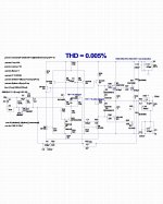
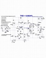
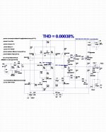
OK, you got 3 versions with THD at 10kHz shown. What really matters most in all of these versions is that source resistors (5W ones) and the Zoebel resistor have the lowest possible inductance. That's why I reduced source resistor values to 0.1 Ohm and that's fine with laterals. I use such values in my ETI477 and resistors are so called non-inductive mpc74.
In Zoebel I use Caddock (mpc74 or KOA bpr58 are good enough) and 100-220nF cap here should also be low inductance polypropylene.
All picofarad caps are and should be silver mica, not ceramics. 220nF and other nF caps are polypropylene as well as the input cap. 10uF is a good compromise here if you want good low frequency response. 330uF cap in nfb is Nichicon Muse BP. Simulation shows that the cap across 22k nfb resistor MUST be 3pF.
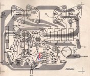
To minimize offset add 1k trimpot as shown in pcb image. You should be able to bring offset down to below 1mV.
In mine eti477 I got rid of the 2nd input HF filter and reduced 1k resistor at the input HF and nfb to 820 ohm to improve stability as I reduced LTP emitter values to 150 ohm to somewhat reduce distortion.
As you see from the attached images THD depends quite a lot on transistors used.
Increasing gate resistors to values shown reduces chances for oscillations and having these higher for N compensates for differences in capacitance of N and P laterals.
cheers,
PS use 1k multiturn trimpots in LTP and to set bias.
In Zoebel I use Caddock (mpc74 or KOA bpr58 are good enough) and 100-220nF cap here should also be low inductance polypropylene.
All picofarad caps are and should be silver mica, not ceramics. 220nF and other nF caps are polypropylene as well as the input cap. 10uF is a good compromise here if you want good low frequency response. 330uF cap in nfb is Nichicon Muse BP. Simulation shows that the cap across 22k nfb resistor MUST be 3pF.
To minimize offset add 1k trimpot as shown in pcb image. You should be able to bring offset down to below 1mV.
In mine eti477 I got rid of the 2nd input HF filter and reduced 1k resistor at the input HF and nfb to 820 ohm to improve stability as I reduced LTP emitter values to 150 ohm to somewhat reduce distortion.
As you see from the attached images THD depends quite a lot on transistors used.
Increasing gate resistors to values shown reduces chances for oscillations and having these higher for N compensates for differences in capacitance of N and P laterals.
cheers,
PS use 1k multiturn trimpots in LTP and to set bias.
Attachments
- Status
- This old topic is closed. If you want to reopen this topic, contact a moderator using the "Report Post" button.
- Home
- Amplifiers
- Solid State
- ETI 477 article