Opamps here. Thing is there is not a virtual ground exactly, rather a virtual offset voltage. There are two outputs for each channel which quiescently rest at 1/2 AVCC, the so-called offset voltage. From there they move differentially for distortion cancellation. So, about 1.65 volts common mode offset for the opamps.
You are very welcome, of course.
Perhaps I should also mention there is an early evaluation board schematic on the same download page. It shows there are two offset voltage signals, one for each channel, each one derived from the conditioned AVCC voltage using two 10k resistors to make a divide-by-two voltage divider, then with a 10uf filter cap on the output.
Perhaps I should also mention there is an early evaluation board schematic on the same download page. It shows there are two offset voltage signals, one for each channel, each one derived from the conditioned AVCC voltage using two 10k resistors to make a divide-by-two voltage divider, then with a 10uf filter cap on the output.
Hi Cdsgames, do you mean decoupling of the opamp, or the DAC-chip itself? It is the DAC-chip decoupling I was referring to. For this, you need more than you can realistically expect from a film cap, 2200 uF or thereabouts.
I mean the decoupling of the dac ic. And I do mean 0.3 Farad (not uF) + film caps on each L and R
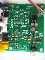
Thought maybe a good idea to post pictures of my particular Chinese DAC in one consolidated place. They mostly show circuits pretty close to what ESS recommends.
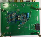
The AVCC circuit is on the bottom of the DAC just under the AVCC filter caps. The resistors on top have been removed. A 3.3v regulator just for analog circuitry is also on the bottom and is the reference for AVCC.
Again on the bottom of the board are four IV circuits. The differential summing amps are on the top of the board where the old voltage output stage used to be.
One picture includes annotations describing components. The annotations are readable if viewed at full resolution.
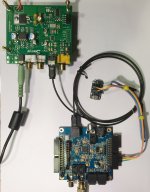
There is also a photo showing the external SRC PCB and Arduino microcontroller for it. Wish I could find an inexpensive alternative that other people could use if they wanted. It really does sound better using Benchmark's scheme of upsampling and using a slow transition minimal phase reconstruction filter. The filter would be audible and not the best choice if there were not an unused frequency band above the 20Hz-20kHz audio content. Currently, the SRC upsamples to 96kHz which provides ample unused frequency headroom above any CD and DVD content.
The AVCC circuit is on the bottom of the DAC just under the AVCC filter caps. The resistors on top have been removed. A 3.3v regulator just for analog circuitry is also on the bottom and is the reference for AVCC.
Again on the bottom of the board are four IV circuits. The differential summing amps are on the top of the board where the old voltage output stage used to be.
One picture includes annotations describing components. The annotations are readable if viewed at full resolution.
There is also a photo showing the external SRC PCB and Arduino microcontroller for it. Wish I could find an inexpensive alternative that other people could use if they wanted. It really does sound better using Benchmark's scheme of upsampling and using a slow transition minimal phase reconstruction filter. The filter would be audible and not the best choice if there were not an unused frequency band above the 20Hz-20kHz audio content. Currently, the SRC upsamples to 96kHz which provides ample unused frequency headroom above any CD and DVD content.
Attachments
Last edited:
I mean the decoupling of the dac ic. And I do mean 0.3 Farad (not uF) + film caps on each L and R
Hi cdsgames, are you referring to the dac ic pins as shown on the first picture I just posted, the annotated one with labels near the AVCC input pins?
By the way, I should probably also mention I made a note at the bottom the annotated picture that says the DAC has a single 1.2 power pin. What I should have said was that there are 3.3v digital power pins, 3.3v AVCC pins, and one 1.2v Vdd pin for the analog output section inside the DAC.
Last edited:
Okay, I see. It turns out ESS recommends using another opamp circuit to provide power there rather than using such big caps. A singe LME49720 and a few small parts likely should do a better job, perhaps at less cost too. The recommended circuit for AVCC is shown on the 4th page of this document:
http://www.esstech.com/files/4514/4095/4306/Application_Note_Component_Selection_and_PCB_Layout.pdf
http://www.esstech.com/files/4514/4095/4306/Application_Note_Component_Selection_and_PCB_Layout.pdf
Yeap ESS recommends low noise , low impedance power for good THD+N measurements . Of course you can use a opamp , but our design choice has the same result. Multiple film caps (and this is after we use 2 LDOs ) will keep the noise undetectable and will decouple the SC and as far as impedance there is nothing better what than having a big reservoir of electrons...right next to the IC
Last edited:
Thank you cdsgames,
Yes supercaps brings something in overal SQ. Better bass and wider airy soundstage... Is it any differences in ESR of using different type of supercaps? Can you put down what kind of supercap did you try? Button caps have esr... 50R or less. Did you use any low esr supercap?
Yes supercaps brings something in overal SQ. Better bass and wider airy soundstage... Is it any differences in ESR of using different type of supercaps? Can you put down what kind of supercap did you try? Button caps have esr... 50R or less. Did you use any low esr supercap?
 Guys - please stop quoting the post right above yours when replying.
Opamps here. Thing is there is not a virtual ground exactly, rather a virtual offset voltage. There are two outputs for each channel which quiescently rest at 1/2 AVCC, the so-called offset voltage. From there they move differentially for distortion cancellation. So, about 1.65 volts common mode offset for the opamps.
Opamps. Mark, thanks for posting the link to the ESS technical page, most helpful.
Great stuff guys, thanks for sharing your development on the boards.
Mark, is the board deriving the 0.5AVCC through a divider network with a capacitor on the lower leg, per convention?
Mark, is the board deriving the 0.5AVCC through a divider network with a capacitor on the lower leg, per convention?
Yes.
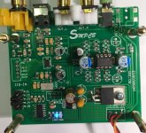
If you would like to see, the two dividers are barely visible in the picture I posted of the solder side of the DAC board.
There is a single LME49720 situated right beneath the two 47uf AVCC capacitors over on the component side, one opamp per channel. That is the AVCC power conditioner.
The tiny PCB attached vertically by one end of the AVCC opamp has two sets of 10k SMD resistor voltage dividers and two 10 uf organic polymer filter capacitor cans you can see from their sides. That is the reference voltage divider.
You can also see there are two reference voltage wires going from the dividers over to the IV stages. All this if you click on the little X in the lower left side of the picture to expand it to full size. (To be clear, I am explaining in a lot of detail for any possibly interested readers who may not be at your level of sophistication. No offence intended.)
- Home
- Source & Line
- Digital Line Level
- ES9038Q2M Board