Regarding NMOS transistors, I was browsing International Rectifier's website. How difficult is it to hand solder a D2Pak or D2Pak 7 Pin package. Is it possible with the drain tab?
There's a lot to choose from even when looking just at one manufacturer...
IRF1324S 1.0mR max Rds(on) D2Pak 7 Pin
IRFS7430 1.2mR max Rds(on) D2Pak, TO-262, TO-247AC, TO-220
IRLS3813 1.95mR max Rds(on) D2Pak
IRF8252 2.7mR max Rds(on) SO-8
There's a lot to choose from even when looking just at one manufacturer...
IRF1324S 1.0mR max Rds(on) D2Pak 7 Pin
IRFS7430 1.2mR max Rds(on) D2Pak, TO-262, TO-247AC, TO-220
IRLS3813 1.95mR max Rds(on) D2Pak
IRF8252 2.7mR max Rds(on) SO-8
Mark already noted that you probably should define your requirements before you do much work, wise words.
With FET Rds down to a few milliohms, or less, that means even with several amp loads that your supply will drop only a few millivolts.
Is this really a problem? As I mentioned, commodity FETS are obtainable with about the same resistance as a reasonable piece of wire.
This is a computer power supply yes?
If you really want instrumentation current sources then you need Kelvin leads anyway.
The 3.3 V rail has an issue with insufficient pull-down so P FETs are not a clear winner.
I like the idea to use N FETs and pull them up, and this reduces Rds problem as well.
Best wishes
David
Hi David
The challenge is defining as one learns. Yes, this is a computer power supply. I thought the task would be simpler, but I am realising there's more involved which isn't necessarily a bad thing.
What I didn't want to implement was a switch that undermined my efforts on a decent regulator setup. It seems to me that minimising Rds(on) and shifting the location of the switch (before the regulators) are sensible decisions to take. I also like Mark's idea of using PGO to open parallel NMOS transistors for the two rails that are most affected by the limited pull-down of the PMOS transistors. It would appear to be very elegant and easy to implement. I can't use PGO high as the trigger for a switch ahead of the regulator. I could look at how to implement FPO low as the trigger for NMOS transistors for the 5V and 3.3V rails - the PMOS implementation was just "easy".
If you really want instrumentation current sources then you need Kelvin leads anyway.
Can you expand on this? There is provision in the ATX spec for Kelvin sense of 3.3V (connection to pin 13 of the 24-pin connector). However, I wasn't planning to take this step in added complexity unless I really should. I was planning on using a LT1084 based regulators with SPX431 as per the discussion here for the 5V and 3.3V supplies. Perhaps introducing Kelvin sensing could be a later project.
Otherwise it's just a case of learning terms, minimising the impact bad ones as much as sensible and within reasonable levels of complexity. Over-engineering is allowed if it contributes to knowledge and also within reasonable levels of complexity. (I'm not building to a budget and if things costs a couple of quid rather than 10s of pounds then I'll add them in.)
I'm hoping that once I am through the current limiting analysis I'm largely done on this part.

Steve
... so P FETs are not a clear winner.
I like the idea to use N FETs and pull them up, and this reduces Rds problem as well.
The complication I see in this is that I don't have ready-to-hand a mechanism for managing in-rush current whereas the AND9093 document from On-Semi describes this for PMOS switches.
It seems to me that an Nchannel source follower, driving a load capacitance with a known upper bound, can be current limited remarkably easily.
Just put a ramp of known dV/dt on the Nchannel's gate, and then trust the gain-of-one source follower circuit to produce that same dV/dt on the source (where the load capacitance is connected). Voila, the load capacitance is driven at a known dV/dt. The capacitor differential equation tells us that
I <= C_upper_bound x dV/dt
As long as your actual capacitance is less than or equal to your estimated capacitance, and as long as your gate waveform is a linear ramp of known dV/dt, the capacitor current (i.e. the MOSFET's Ids) is known and bounded. Boom, done.
edit: Or, use miller effect feedback on a common-source connected PMOS {as ON Semiconductor's app note suggests}, and don't switch on the parallel NMOS until hundreds of milliseconds later, long after the inrush current event is complete.
Last edited:
I was about to answer my own question having done more reading:
- fixed pull-up current on gate (Ipu)
- capacitor from gate to ground (Cgate)
- to limit in-rush current (Iirmax) set
Cgate = Cload x Ipu / Irma
P41 http://m.powerelectronics.com/site-...lectronics.com/images/PETInnovations-1110.pdf
I was just now thinking about how the pull up current can be managed easily with VOM1271s in place. For now I'm leaning towards the strategy you added in italics. I will have a go at the circuit tomorrow (fixing the error in my previous circuit and adding the PGO trigger for 12V to a NMOSFET on each of the 5V and 3.3V supplies). I will also take a look at a circuit with VOM1271 an N-channel FETs with the current limiting mentioned above.
Last edited:
SGK,
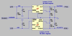
Sorry to confuse the design even more, but have you considered using voltage regulators that have an enable function. I am thinking of the LT1963a which is available in an adjustable version (for +12v and +5v) and a fixed 3.3v version. The enable pin should be pulled up to its supply voltage with a 100k resistor (that's what I used). If all the input voltages are within spec, then turn on the regulators. See attached details.
I recently used the LT1121 and LT1175 in so-8 packages for a small power supply, and they worked very well. The LT1963a is a bigger version of the LT1121. They even have thermal shutdown (just don't touch the package after they shutdown - it hurts).
Note that the enable input pin is internally limited to +7v, hence the 100k pullup resistor. You could use a number of LM393 comparators to pull the enable pins down until all input voltages are correct.
Paul Bysouth
Attachments

I'm sorry Paul, I missed the email notification of your post. I'm not planning to use a regulator with an enable function. I was planning to use a regular with an LT1084 and SPX431 at its core, as discussing in this thread. It's a shame it's not as good as the LM317+SPX431.
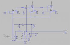
I am prepared to admit I must be a dunce. I spent a couple of hours this evening trying to implement the logic of PGO high turning on the parallel N channel FETs and for PGO low to turn them off. I'm sure this is incredibly easy but I'm not getting it. I will have another go tomorrow. At 12.30am it's time to call it a defeat for this evening.
Attachments
SGK,
How's this for an idea - see diagram. Use a P channel mosfet for the +12v rail (pull gate to ground to turn on), and N channel mosfets for the +5 and +3.3v volt rails (the 10k resistors pull the gates up to +12v to turn them on). The N channel mosfets should be very low Rds on mosfets, the +12v P channel mosfet shouldn't be so critical.
Note the use of a dual open collector comparator as the drivers. The LM393 is half the price of a single small mosfet and you get two if them in a package!
Alternatively you could use a vom1271 to drive the +12v rail mosfet (which could then be an N channel mosfet), and use the lm393 to provide the 20mA drive current. Or better still use two lm393's to each drive about 12mA into the vom1271 opto voltaic driver.
Regards,
Paul Bysouth
Attachments
Hi Paul
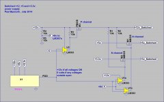
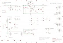
Thanks for the above. I've never looked at comparators before and so I did some reading today. In the end, however, I decided this was getting unnecessarily complicated and so I opened a clean schematic and focused on FPO going low to turn on a 5V supply. I think the below works. I want to spend more time on the current limiting but I think the logic of the power rail turn-on works. I'm also cognisant of the fact that each voltage rail will be a different pcb board and I want to minimise wires running between the rail boards (to and from the 5VSB/control board is fine/unavoidable).
Sorry Mark, in the end - if I can get the current limiting to work properly with this circuit - the parallel setup was getting messy for me and I was struggling to get the voltage drivers to work properly (although perhaps if I revisited after doing the below I may find it easier than late last night).
I would appreciate any comments/corrections/alerts to problems etc.
Once again, thanks for all the help given here already.
Regards
Steve
Attachments
Thanks! I still have a few questions before giving this a go.
I'm still unsure I have the current limiting setup correctly (and the right calculation for the gate capacitor).
Is there a recommended methodology for determining bleeder resistors to discharge voltage rail capacitors?
How difficult is it to hand solder a D2Pak or D2Pak 7 Pin package. Is it possible with the drain tab? I want to learn how to do "skillet SMD soldering" but would like to be able to fall back to hand soldering if I find I am mess in things up. This will help me choose the NMOS transistors (IRF1324S 1.0mR max Rds(on) D2Pak 7 Pin; IRFS7430 1.2mR max Rds(on) D2Pak, TO-262, TO-247AC, TO-220; IRLS3813 1.95mR max Rds(on) D2Pak, TO-220AB; IRF8252 2.7mR max Rds(on) SO-8 etc.)
Lastly, for small signal wiring such as to the VOM1271 and back from the 2N7002, is something like cable stripped from the inside of an Ethernet cable suitable?
Thanks in advance
Steve
I'm still unsure I have the current limiting setup correctly (and the right calculation for the gate capacitor).
- Am I right to understand that once the gate capacitor is charged there's no throttle control on the current through the switch?
- Next we're talking milliseconds here and so, if the foregoing is correct, being conservative re estimating load capacitance and the size of the gate capacitor has trivial consequences? (I note that it is recommended that the 5V and 3V3 come up to 75% voltage within 20ms although there is no requirement to do so. There are also recommendations as to how quickly these voltages should fall below 75% when PGO goes low.)
Is there a recommended methodology for determining bleeder resistors to discharge voltage rail capacitors?
How difficult is it to hand solder a D2Pak or D2Pak 7 Pin package. Is it possible with the drain tab? I want to learn how to do "skillet SMD soldering" but would like to be able to fall back to hand soldering if I find I am mess in things up. This will help me choose the NMOS transistors (IRF1324S 1.0mR max Rds(on) D2Pak 7 Pin; IRFS7430 1.2mR max Rds(on) D2Pak, TO-262, TO-247AC, TO-220; IRLS3813 1.95mR max Rds(on) D2Pak, TO-220AB; IRF8252 2.7mR max Rds(on) SO-8 etc.)
Lastly, for small signal wiring such as to the VOM1271 and back from the 2N7002, is something like cable stripped from the inside of an Ethernet cable suitable?
Thanks in advance
Steve
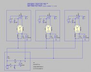
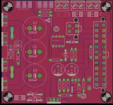
Some progress. 5VSB and power management board. I still have a few things to tidy up. The board is 8x8cm. Regulation is overkill for a standby supply but 'what the hell' and I can now copy and paste chunks when I do the power rails.
Any constructive comments appreciated as this is only the second board I have done.
Steve
Any constructive comments appreciated as this is only the second board I have done.
Steve
Attachments
the gate voltage controls the current through the D to S channel.Am I right to understand that once the gate capacitor is charged there's no throttle control on the current through the switch?
I presume that's what you mean by throttle.
If the circuit needs to adjust the current to a new value the control voltage has to change. That change will require the voltage on the gate capacitance to change. That means charge current is pushed in or pulled out.
The SPEED of the change determines how much current is required into or out of the gate.
I said way back that SPEED was the important factor.
Very slow changes needs virtually no current.
Very fast changes need surprisingly high currents.
Will you want to charge up 1nF of gate capacitance from 3V to 4V in 10ns, compared to wanting to charge 1nF from 3V to 4V in 2s?
what are Kelvin micro Farads?
thousand. I will change it to lower case.
the gate voltage controls the current through the D to S channel.
I presume that's what you mean by throttle.
If the circuit needs to adjust the current to a new value the control voltage has to change. That change will require the voltage on the gate capacitance to change. That means charge current is pushed in or pulled out.
The SPEED of the change determines how much current is required into or out of the gate.
I said way back that SPEED was the important factor.
Very slow changes needs virtually no current.
Very fast changes need surprisingly high currents.
Will you want to charge up 1nF of gate capacitance from 3V to 4V in 10ns, compared to wanting to charge 1nF from 3V to 4V in 2s?
I'm referring to the caps from gate to ground on each of the pass transistors (one per rail). The addition and charging of these is intended to limit/throttle the in-rush through the pass transistor. (I do understand the the transistor gate capacitance is small.) From the link I provided above pg 41), I understanding that adding the cap allows the gate of the FET to be slowly enhanced with a constant change in voltage "and when this voltage exceeds the gate threshold, the source rises at the same slew rate." I understand the VOM1271 (represented by PC817A in the LTspice schematic) will provide the constant current required. I can't model this side of things as there is no Spice model available for the VOM1271.
My own personal preference is to spend the necessary time to create personalized "components" (the KiCad name for PCB layout entities), so that I can tweak them in various minor ways, and satisfy my own idiosyncratic goals. On this board, I might consider
- Changing the layout of "big electrolytic cap" (C1-C3) so that both the bottomside and topside silkscreen indicate the positive terminal. And, since there appears to be plenty of room, I'd make a second topside polarity indicator which is still visible after the physical capacitor is installed and soldered.
- Changing the silkscreen of the 8 pin TPS3510 to include a more pronounced orientation "notch" and/or "pin 1 heavy dot"
- Making the reference designators for J5 and J6 visible. On the present layout these are mystery devices.
- Sliding R8-R9-Q1 to the southeast (towards LED1) and relieving the unnecessary congestion near C1.
- Adding test points (1-pin "connectors", i.e. scope probe attachment points) at pins C and R of the SPX431 IC ... so that one day you are able to see for yourself just how stable it really is under 1% - 99% square wave Iload testing. Even if you never perform these tests, it's reassuring to know that you could, if you really wanted to.
Thx. I haven't done the silkscreen yet - I have a script which generates it from various layers - but I have made the first 3 changes you suggested in text which will end up in the silkscreen. Re the fourth, I have shifted the parts a little but remember the 3V3 trace and cap C10 are on the bottom of the board.
For the test connectors, do you mean breakaway headers like these and 0.8mm wire pad holes to fit them in?
How does one generate the square wave Iload for testing?
For the test connectors, do you mean breakaway headers like these and 0.8mm wire pad holes to fit them in?
How does one generate the square wave Iload for testing?
- Status
- This old topic is closed. If you want to reopen this topic, contact a moderator using the "Report Post" button.
- Home
- Amplifiers
- Power Supplies
- Enough current to turn on 3 mosfets?