SGK,
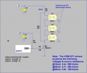
The IRFB3077 mosfet has a high input capacitance (~9nF) so it will need a reasonable amount of current to charge this gate capacitance up to get the mosfet to turn on. The vom1271 will produce sufficient voltage (~8.5v if the datasheet is to be believed), but its effective source resistance is very dependent on the LED current. I would drive the vom1271s LEDs (in series) at 20mA to 25mA of current. See attached diagram for my suggestion.
Paul Bysouth
Attachments
SGK,
The IRFB3077 mosfet has a high input capacitance (~9nF) so it will need a reasonable amount of current to charge this gate capacitance up to get the mosfet to turn on. The vom1271 will produce sufficient voltage (~8.5v if the datasheet is to be believed), but its effective source resistance is very dependent on the LED current. I would drive the vom1271s LEDs (in series) at 20mA to 25mA of current. See attached diagram for my suggestion.
Paul Bysouth
+100%
I was just reading the TPS3510 datasheet and came to the same conclusion.
Cheers ,
Rens
Paul/Rens
Thanks for this.
Perhaps I am mistaken but I don't think PGO can be pulled up from the 12V supply. The max recommended voltage in the datasheet for PGO is 7V and the ATX spec calls for a 5V (TTL compatible) signal to the motherboard (from PGO). The TPS3510 can sink up to 10mA maximum through PGO when held low.
The TN2510 has a low Vgs(th) of 2V which would seem to be good. I need to track down a Spice model for the TN2510. If V1 is 5V and R1 500 ohms (R3 removed) Vgs is 5V, as Andrew has noted little current is needed to charge the gate, your use of R2 and R4 means Vds is still 5V... It seems all ok, no? Is my logic/analysis correct?
Regards
Steve
PS: I keep thinking about how to have PSON be the driver of the rail switches but it would seem that using this as the trigger (PSON pulled low by the motherboard) would require more complex TTL programming.
Since there is only one "ground" for the entire circuit, and the photovoltaic couplers are not being used for galvanic isolation of two independent subsystems with different "grounds" ...
It seems to me you could save a lot of money on parts by building a straightforward, DC coupled signal booster. Just a logic inverter with level shifting. Use the 5V digital signal "PGO" on TPS3510 pin#8, to create a 12V digital signal "12V_PGO_inverse" with a very low output impedance / very strong output drive.
Then you use "12V_PGO_inverse" to drive the gates of three Pchannel MOSFET pass transistors. You're only passing 5.0 amperes of current; for that, you can fit the very low-cost SMD device IRF9317. Its dissipation will be IxIxR = 5x5x0.007 = 175 milliwatts, well within the device ratings even when the ambient air is 70 degrees C. And it's in the SO-8 gullwing package which is quite easily hand-soldered; there's no ground-slug beneath the package body that requires oven-reflow soldering.
You don't need to pay for expensive photovoltaic drivers, you don't need to pay for expensive 1 milliohm FETs, and you don't need to drive high capacitance from a scrawny TPS3510 5V digital output pin.
In this arrangement, the weakest link will be the 3.3V pass transistor, since it has the least Vgs. If that frightens you, and it shouldn't (see Figure 1 of the IRF9317 datasheet), just connect two (or more) pass transistors in parallel. This reduces Rds_on by a factor of N, which reduces the voltage drop across the composite switch by the same factor of N.
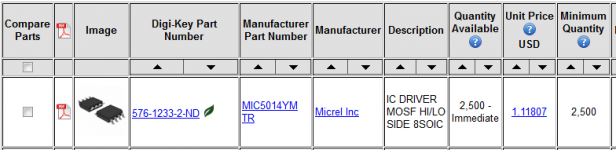
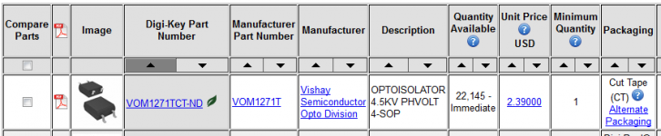
Or, if you absolutely insist upon using big, expensive, thru-hole Nchannel pass transistors ("high side switches"), you could buy high side switch driver ICs for a lot less money than photovoltaic isolators. The Micrel MIC5014, with on-chip charge pump, is one possibility. Price is 50% less than VOM1271 photovoltaic isolator AND it was purpose-built by expert designers, to drive a big whomping MOSFET.
It seems to me you could save a lot of money on parts by building a straightforward, DC coupled signal booster. Just a logic inverter with level shifting. Use the 5V digital signal "PGO" on TPS3510 pin#8, to create a 12V digital signal "12V_PGO_inverse" with a very low output impedance / very strong output drive.
Then you use "12V_PGO_inverse" to drive the gates of three Pchannel MOSFET pass transistors. You're only passing 5.0 amperes of current; for that, you can fit the very low-cost SMD device IRF9317. Its dissipation will be IxIxR = 5x5x0.007 = 175 milliwatts, well within the device ratings even when the ambient air is 70 degrees C. And it's in the SO-8 gullwing package which is quite easily hand-soldered; there's no ground-slug beneath the package body that requires oven-reflow soldering.
You don't need to pay for expensive photovoltaic drivers, you don't need to pay for expensive 1 milliohm FETs, and you don't need to drive high capacitance from a scrawny TPS3510 5V digital output pin.
In this arrangement, the weakest link will be the 3.3V pass transistor, since it has the least Vgs. If that frightens you, and it shouldn't (see Figure 1 of the IRF9317 datasheet), just connect two (or more) pass transistors in parallel. This reduces Rds_on by a factor of N, which reduces the voltage drop across the composite switch by the same factor of N.
Or, if you absolutely insist upon using big, expensive, thru-hole Nchannel pass transistors ("high side switches"), you could buy high side switch driver ICs for a lot less money than photovoltaic isolators. The Micrel MIC5014, with on-chip charge pump, is one possibility. Price is 50% less than VOM1271 photovoltaic isolator AND it was purpose-built by expert designers, to drive a big whomping MOSFET.
Since there is only one "ground" for the entire circuit, and the photovoltaic couplers are not being used for galvanic isolation of two independent subsystems with different "grounds" ...
Oh, this had been needling my conscience for awhile. But I ignored it, unsure and thinking I was in sight of a workable solution even if it was inefficient and not cost effective.
It seems to me you could save a lot of money on parts by building a straightforward, DC coupled signal booster. Just a logic inverter with level shifting. Use the 5V digital signal "PGO" on TPS3510 pin#8, to create a 12V digital signal "12V_PGO_inverse" with a very low output impedance / very strong output drive.
Then you use "12V_PGO_inverse" to drive the gates of three Pchannel MOSFET pass transistors. You're only passing 5.0 amperes of current; for that, you can fit the very low-cost SMD device IRF9317. Its dissipation will be IxIxR = 5x5x0.007 = 175 milliwatts, well within the device ratings even when the ambient air is 70 degrees C. And it's in the SO-8 gullwing package which is quite easily hand-soldered; there's no ground-slug beneath the package body that requires oven-reflow soldering.
You don't need to pay for expensive photovoltaic drivers, you don't need to pay for expensive 1 milliohm FETs, and you don't need to drive high capacitance from a scrawny TPS3510 5V digital output pin.
In this arrangement, the weakest link will be the 3.3V pass transistor, since it has the least Vgs. If that frightens you, and it shouldn't (see Figure 1 of the IRF9317 datasheet), just connect two (or more) pass transistors in parallel. This reduces Rds_on by a factor of N, which reduces the voltage drop across the composite switch by the same factor of N.
I put this in the same basket as my "PS" in my last post. I don't know where to start but I will begin investigating.
Or, if you absolutely insist upon using big, expensive, thru-hole Nchannel pass transistors ("high side switches"), you could buy high side switch driver ICs for a lot less money than photovoltaic isolators. The Micrel MIC5014, with on-chip charge pump, is one possibility. Price is 50% less than VOM1271 photovoltaic isolator AND it was purpose-built by expert designers, to drive a big whomping MOSFET.
Maybe this is an interim solution.
This is exhausting...but I am learning with the help of you guys. much appreciated.
Cheers
Steve
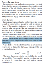
I had about an hour this evening to do a bit more reading and came across this article Using MOSFETs in Load Switch Applications. Fig 3 would seem informative with EN replaced by PGO. What might be a suitable small-signal NMOS transistor for Q1 and what would be the disadvantages of this versus your proposal of a DC coupled signal booster?
I note also the article's comments regarding the impact of Rds(on) on output voltage and its load dependency, and the noted disadvantage of P-channel MOSFETs in this regard. Is it worth worrying about this?
With respect to the common ground, I went back to Piisami's circuit which provided the original inspiration for my suggested use of VOM1271. Isn't the same point applicable here i.e. common ground for +ve, -ve and the circuit providing the control voltage?
(I realise this is likely even more exhausting for you guys to teach me this stuff…)
If you discard photovoltaic optoisolators, and if you confine yourself to BJTs, JFETs, MOSFETs, resistors, capacitors, diodes, ICs, and inductors, these are native elements in LTSPICE. Which means that you can try out your circuit design in simulation and see, with your own eyes, exactly how well it performs. If adequate, rejoice. If not adequate, redesign and resimulate.
It's probably a good idea to decide upon your important objectives, and your "that's plenty good enough for me" stopping criteria, lest you waste a lot of time needlessly polishing a coprolite. I suspect that "at max load current, input to output delta-V shall be less than WXYZ microvolts" might be one of your objectives.
It's probably a good idea to decide upon your important objectives, and your "that's plenty good enough for me" stopping criteria, lest you waste a lot of time needlessly polishing a coprolite. I suspect that "at max load current, input to output delta-V shall be less than WXYZ microvolts" might be one of your objectives.
Agreed and thank you. I would like to understand better the common ground point and why the decision to use photovoltaic MOSFET drivers in Piisami's circuit. Sounds like there were other objectives driving that decision which may not be applicable here. So that may well have been a wild goose chase albeit a learning experience.
On p versus n mosfets, I at least have a better appreciation of the impact of Rds(on) now. I have voltage rails available and so if there is a n equivalent of the p channel MOSFET you mentioned but with appreciably lower Rds(on) then maybe that's worth using.
For Q1 in the paper I linked to, i will for now explore using the transistor Paul used unless there are better suggestions.
I will also try to learn more about your doc coupled signal boosters. Thanks again.
I would like to understand better ...why the decision to use photovoltaic MOSFET drivers in Piisami's circuit.
For power amplifier circuits like Piisami's, there is a need to break supply lines of both polarities simultaneously, and with fairly substantial currents and volts.
The desire to reduce losses at that current level tends to push towards N Fets in both supply lines. The supply rails are above the 30V limit of the MICREL 5014 (is this easy to work-around?).
And you have some handy extra rails.
So trade-offs aren't quite the same.
On the other hand, I don't know where Mark Johnson has his prices from, perhaps better than my on-line lazy choice.
Mouser shows the Micrel 5014 as just a little more expensive than the VOM1271 rather than cheaper. And "expensive photovoltaic drivers" ? Mouser price is less than $4 each. So photovoltaic is hardly a bad solution, even if you need three.
Probably more a case of choose what you find convenient.
Best wishes
David
Last edited:
I'm not chomping at the bit to use photovoltaic Mosfet drivers if they don't offer compelling benefits. I had thought it advisable (and I was thinking isolation was the driver of their use in the amp PSU even though I doubted this due to the common ground), but it seems in this case they're a waste of space. If they can be dropped then it seems things would appear to get simpler fast. As Andrew has said a few times, I don't need much current.
I could probably use a circuit like Fig 3 in the article I linked to: PGO goes high presenting 5V to the gate of a low-current/small signal NMOS transistor which turns on, the gates of 3 P-channel load switches (1 per voltage rail) go to ground and the switches turn on. Or, could I not use the small signal NMOS transistor as a high-side switch to present 12V to each of the gates of 3 N-channel load switches when PGO goes high and turns it on, thereby turning on the load switches. I will try to model each this weekend.
On the PMOS versus NMOS decision, my hesitation here - quite probably ill-founded - is that even though this is a low-current application versus a power amp, a variable load induces volatility in Vout. If the only cost of NMOS is equialent to a pint of beer and the slightly extra space of TO-220 (NMOS) versus SO-8 (PMOS), why not opt for the NMOS setup given the 12V rail is available? Unless, of course I am missing something re the high-side setup...
Cheers
Steve
I suspect that "at max load current, input to output delta-V shall be less than WXYZ microvolts" might be one of your objectives.
I suspect that your objectives might also include "I will simulate a start-up event with max load current and also max bypass capacitance at the load (after the switch). My design shall limit the peak inrush current to ABCD amperes and it shall limit the peak instantaneous power dissipation (P = Ids x Vds) to JKLM watts. During start-up my power-switch devices shall remain within their Safe Operating Area, presented on the datasheet"
Attachments
Alright, I think I have - finally - got my head around a few things including high-side versus low-side switching, the challenge associated with high-side switching and NMOS transistor switches, NMOS vs PMOS Rds(on) characteristics, Vgs etc. I know I have been slow.
In this make-shift structure I am proposing the switches will be after the regulation
circuits.
Hence it seems to me that one ought to be concerned about the impact of Rds(on) on the rail voltages. The regulation circuit boards endeavour to produce good stable voltages and then there's a switch after them which swings voltage with load. Perhaps this poor structure means it really is a coprolite.
The proper answer would be to place the switches before the regulation (making note to manage the in-rush due to at least the regulation output caps) but then I can't use PGO as the simple "trigger" and I would need a proper 5V standby circuit as opposed to using the main 5V. The latter isn't such a big deal but when I look at the spec for PSON I'm not sure where I would start.
In this make-shift structure I am proposing the switches will be after the regulation
circuits.
An externally hosted image should be here but it was not working when we last tested it.
Hence it seems to me that one ought to be concerned about the impact of Rds(on) on the rail voltages. The regulation circuit boards endeavour to produce good stable voltages and then there's a switch after them which swings voltage with load. Perhaps this poor structure means it really is a coprolite.
The proper answer would be to place the switches before the regulation (making note to manage the in-rush due to at least the regulation output caps) but then I can't use PGO as the simple "trigger" and I would need a proper 5V standby circuit as opposed to using the main 5V. The latter isn't such a big deal but when I look at the spec for PSON I'm not sure where I would start.
An externally hosted image should be here but it was not working when we last tested it.
Last edited:
Possible solution with PMOS transistor switches placed after the input caps but before the regulators of each supply rail (other than V5SB)? FPO going low becomes the trigger. FPO can sink up to 20mA (and rated to 15V). When FPO goes high the pass transistors turn off.
In-rush for at least the supply output caps would have to be managed. Presumably the regulators will do their best to correct for the transistor resistance. Rdson is particularly an issue for the 3V3 rail as Vgs is lower. The IRF9310 would seem to have slightly better specs in this regard than the IRF9317 but the problem remains. Of course the rail voltages ahead of the regulators will be higher than shown here and hence Vgs better.
Less of a coprolite?
Below is an excerpt from the TPS3510 data sheet covering PSON and FPO.
An externally hosted image should be here but it was not working when we last tested it.
I glanced at a couple of ATX motherboards and counted about 60 electrolytic bypass capacitors on the busiest of the bunch. Making a conservative over-estimate that each electrolytic cap is 220 microfarads {balderdash!}, and they are all on the same power supply rail {but we don't know which one!!} that's 13.2 millifarads for an inrush current limiter to drive.
Assuming the inrush current must be limited to 5.0 amperes or less, then I = C x deltaV/deltaT says that
The delayed signal(s) can activate a second, parallel, power MOSFET to lower the switch resistance. And the second MOSFET can a be surface mounted Nchannel device for the 5.0V and 3.3V supplies, since 12V on the gate is plenty high enough to turn an NMOS on when Vsource = 5 or 3.3v. Recalling that the 3.3V supply is the weakest of the three (least Vgs), we observe that the extra NMOS is being applied where it is needed the most.
Assuming the inrush current must be limited to 5.0 amperes or less, then I = C x deltaV/deltaT says that
- deltaT >= 8.7 milliseconds for the 3.3 volt supply
- deltaT >= 32 milliseconds for the 12 volt supply
The delayed signal(s) can activate a second, parallel, power MOSFET to lower the switch resistance. And the second MOSFET can a be surface mounted Nchannel device for the 5.0V and 3.3V supplies, since 12V on the gate is plenty high enough to turn an NMOS on when Vsource = 5 or 3.3v. Recalling that the 3.3V supply is the weakest of the three (least Vgs), we observe that the extra NMOS is being applied where it is needed the most.
Last edited:
Hi.
PGO is already delayed 300ms after the voltage signals for PGI, VS33 and VS5 go above their under-voltage thresholds. If I read the TPS3510 data sheet correctly:
- FPO goes low 40.3ms after PSON goes low
- in my circuit, if it works, FPO low turns on the supply rails
- PGI/3.3v/5v/12v ramp up through their under-voltage thresholds
- 300ms later PGO goes high
So…if I understand you correctly, even adjusting your timing calculations for large output caps on each voltage rail (post switch in my latest typology), I suspect a delayed PGO may not be needed. (What's not clear to me is whether the mobo capacitance charges before the mono receives PGO but let's keep your numbers in the calculation for safety.) Or am I missing something?
It's just a few crazy thoughts
- guesstimate the post-switch load capacitance: how?
- what to do AFTER the soft-start, inrush-current-limited capacitor charge-up has completed?
- possible inclusion of Nchannel switch in parallel with Pchannel switch, on low-Vout {hence low-Vgs} supplies?
...concerned about the impact of Rds(on) on the rail volt...
Mark already noted that you probably should define your requirements before you do much work, wise words.
With FET Rds down to a few milliohms, or less, that means even with several amp loads that your supply will drop only a few millivolts.
Is this really a problem? As I mentioned, commodity FETS are obtainable with about the same resistance as a reasonable piece of wire.
This is a computer power supply yes?
If you really want instrumentation current sources then you need Kelvin leads anyway.
The 3.3 V rail has an issue with insufficient pull-down so P FETs are not a clear winner.
I like the idea to use N FETs and pull them up, and this reduces Rds problem as well.
Best wishes
David
Last edited:
- Status
- This old topic is closed. If you want to reopen this topic, contact a moderator using the "Report Post" button.
- Home
- Amplifiers
- Power Supplies
- Enough current to turn on 3 mosfets?