Congratulations Phil,getting nearer to perfection with each iteration.
Actually, amplifiers sharing this topology resemble Mr. Self's Blameless
in their pursuit for perfection.I believe he has done a great work for this
community.
This time, I have an advice list and a question list.Here comes the advice list
first:
1.Don't use the 30R trimmer in the emiiter legs of the LTP.With a small effort
in matching, the output offset will be in the few mV range and you won't
need to zero it down.In the long term, trimmers, especially the open types,
will prove to be more harmful than helpful.Just use good old fixed R's about
100R each.
2.Divide the 6K8 R to 3K3 + 3K3 for the bias of the CCS's and connect a cap
between their junction and the + supply.
3.Replace the 29K R on the input of the amp with a 22K R if you want to keep
the 6K8 & 470p low pass filter.This will make the bias current caused voltage
drop similar to the one through the feedback R.
4.The Vbe multiplier should have a fixed R between the collector & base and
the trimmer should be between base & emitter in series with a limiting R.
5.Use base stopper R's for the predrivers in the range 47R to 220R
6.Increase the VAS current somewhat.Maybe 10mA.
7.Use low value R's (0.1R to 0.22R) in the emitter legs of the outputs.
Now, the question list for the more knowlegeable ones among us:
1.Why don't people use R/C filters in bases of the CCS transistors?A very
big time constant created this way will eliminate the switch on thump.
2.I remember reading about the feedback cap being formed by connecting
2 similar ones in parallel but poles interchanged.This configuration,
according to the author of the thread,was the most preferred one.Please
post your opinions on this subject.
Keep up the good work Phil.
Cheers
Selim
P.S. PCB's will be on their way shortly.
Hey you two - most wonderful indeed. I feel like I am making some progress, which is amazing considering I had trouble making a piece of nichrome hot, a few years back. The nichrome wire was part of a 'bow' that I made to cut out a couple of model airplane wings. I can remember it took me a week or two just to build a power supply, and I was compelled to learn (by heart) Ohm's law. That small piece of knowledge (volts = amps x ohms) was a major break-through for me, and I was chuffed.
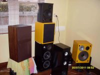
I have been spray-painting a few speaker boxes that I have built and will post a picture. Paint has a wonderful orange-peel texture to it, but I have grown to live with this aesthetic! Zero degrees or below down here in the evenings, so paint will not spray properly unless you have a warm place to do the job, and cure the paint.
Selim & Ingenius, I will follow all the instructions posted and thankyou for being so specific. It is important to fellows like me to get that kind of help, because we only know a little bit. Remember what I said about Ohm's Law?
Some-times contributors like yourselves have to give all the information at the risk of 'appearing' patronising; - But, you fellows know that this it is a small price to pay, in order to see the smitten smile of an otherwise miserable man; and YES I am smiling now.
Bread-board is next, then I can read all the voltages and currents and take a look at some waves on my old (once again salvaged) 50Mhz scope!
Attachments
I agree all this advice.1.Don't use the 30R trimmer in the emiiter legs of the LTP.With a small effort
in matching, the output offset will be in the few mV range and you won't
need to zero it down.In the long term, trimmers, especially the open types,
will prove to be more harmful than helpful.Just use good old fixed R's about
100R each.
4.The Vbe multiplier should have a fixed R between the collector & base and
the trimmer should be between base & emitter in series with a limiting R.
5.Use base stopper R's for the drivers in the range 47R to 220R. There are no pre-drivers.
6.Increase the VAS current somewhat.Maybe 10mA.
7.Use low value R's (0.1R to 0.22R) in the emitter legs of the outputs.
I would recommend reducing the 6k8 rather than reducing the 29k at the input.
Remove the emitter resistors from the two protection transistors.
Getting Warmer Already - Like BB. Kings Guitar.
Hello again.
Did the adjustments and a few more, I reckon it's close but will need further scrutiny & advice, please bear with me because I feel like you have almost got it.
Very happy man
Hello again.
Did the adjustments and a few more, I reckon it's close but will need further scrutiny & advice, please bear with me because I feel like you have almost got it.
- I'm unsure about the diodes over the collector-emitter of output devices. Can this interfere with the normal operation of the amps?
- I have put 0.47 Ohm - 5W resistors in both the collector and emitter of the output transistors. Is this too large? I have 200VA per channell, if this has a bearing on the selection.
- Are the base resistors a good or bad idea on the output transistors?
- I have four brand spanking new Phillips 4700/63V electrolytic caps so I thought I would stick them on the amp board itself so that the output devices are not poaching power from the rest of the circuit. Is this ok?
- I am planning a very big aluminium box for this and future amp projects so I will make room inside for everything.
- Did I get the Vbe multiplier in the bias right? Probably not - I want to see what the difference is between A & AB weighting. (If that's the word & if it is actually that simple).
- Do we have a sufficient amount of juice flowing through the differential pair now?
- Have I gone over the top again, with those caps on the rails; Looks a bit heavy duty but I have so many good HV caps I just wanted to use a few! But if no good - they'll have to go.
- I am still using the A970/C2240 D669/B649 & C4468/A1695 devices on this board. But I want the other readers to know that I acknowledge the superior components such as the C3281/A1302, MJE340/350, MPSA92, 42 & 06 and so on etcetera. I have already looked into these and other devices and they appear to be very good value for money. I will substitute the better devices into my next amp.
Very happy man
Attachments
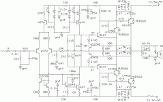
Here is my take on the changes suggested by selim. I can't quite get the collector current in the drivers up to 10mA without worsening the THD. It's now 5mA and 7mA.
For the collector resistors, I have used two 0.22 ohm in parallel. This makes it possible to get away with 5W devices.
It still looks good, with THD now at 0.006%.
I haven't checked the workings of the VI limiter yet.
For the collector resistors, I have used two 0.22 ohm in parallel. This makes it possible to get away with 5W devices.
It still looks good, with THD now at 0.006%.
I haven't checked the workings of the VI limiter yet.
Attachments
Last edited:
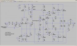
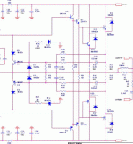
Hi ingenieus,
Thanks a lot for your efforts in perfecting this amp.The schematic you have
posted is almost exactly what I had in mind.Could you please give the
simulator one more run with the following changes:
1.As an approximation to AndrewT's recommendation,change the value of
R12 from 22K to 27K and the value of R11 from 6K8 to 2K2
2.Mr.Self advocates the use of heavy degeneration for the LTP for better THD
performance.So the values of R7 and R8 might be increased to 100R or 150R.
3.To increase the VAS current,the value of R6 might be reduced from 220R to
56R.
4.Finally, 0R22 resistors might be added in series with the emitters of Q1,
Q14, and Q2, Q15.
If there is any improvement at all, then I think we have reached the limits
of this topology.Of course,further simulations should be done for the sake of
optimization before reaching out for the solder.Main points to consider are
the tail current for the LTP and the VAS current.
Once again, thanks very much for your efforts.
Cheers
Selim
What language is that? I like it.
I understood the THD acronym but man, you guys really talk a different language amongst yourselves don't you! Chuckle, Chuckle.
I'm going to Tech next year so I can learn me some of that vernacular.
I downloaded Linear Tech program and will try to get it percolating tonight.
Itching to get that amp on the breadboard & it wont be long now.
Very excited, haven't stoped bouncing around the workbench today. Digging out caps and resistors - even got a few spare bits of photo-sensitive board to put it on.
Bob Cordell shows how to calculate the degeneration effect of the different values of emitter resistor. From there he shows how to calculate the open loop gain (OLG).
Once that has been established then stability becomes an easier problem to overcome.
Simply changing the emitter resistor without knowledge of how that change affects OLG is guessing at stability criteria.
Once that has been established then stability becomes an easier problem to overcome.
Simply changing the emitter resistor without knowledge of how that change affects OLG is guessing at stability criteria.
Bob Cordell shows how to calculate the degeneration effect of the different values of emitter resistor. From there he shows how to calculate the open loop gain (OLG).
Once that has been established then stability becomes an easier problem to overcome.
Simply changing the emitter resistor without knowledge of how that change affects OLG is guessing at stability criteria.
HI there Andy, I visited Bob Cordells site, Haven't found that article yet, but will keep trying. Did you see his THD analyser?
Thanks again, Phil
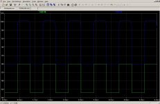
Will need to have another look at the output stage, as the VI limiter only kicks in for the positive half of the output. In the negative half of the output waveform, current goes up to 60A and beyond in my simulation! The voltages and currents that this circuit is capable of should be taken seriously.
Also, according to Randy Slone, those 0.22 ohm resistors should be on the emitter side of the output transistors. They help to balance out minor variations in Vbe among the parallel devices. A Spice simulation does not model this, but it is there in the real world. Waiting to turn an audio amplifier into an arc welder. It will be brief but spectacular when it happens.
Also, according to Randy Slone, those 0.22 ohm resistors should be on the emitter side of the output transistors. They help to balance out minor variations in Vbe among the parallel devices. A Spice simulation does not model this, but it is there in the real world. Waiting to turn an audio amplifier into an arc welder. It will be brief but spectacular when it happens.
VI limiting
Sorry about the big text - I'm using a very small computor monitor.
According to Phil Anderson and Rod Elliott this is a problem that a lot of commercial designs suffer from. And yet people that use these designs still manage to operate their amp within it's limits.
These guys went on to describe a test which will show if a finished amp has inherant problems - But no solution was described. I was left feeling like a man had just been told me I am going to die, "but at least it will be quick" - something like 30ms.
I know that the waves we are dealing with are assymetrical so in theory any limiting should be on both halves of the circuit.
I have also noticed that quite a few designs have no more than a fuse on the output.
The Low Leach TIM3A has an interesting arrangement that is said to be "complete".
Attachments
Here is another take on the circuit, this time with VI limiter in place. It needed an active load for the VAS to make it work. There is a trade-off between limiting the short-circuit current and performance into a 4 ohm load. Too much protection hurts the voltage swing available. As it stands it will give 150W into 8 ohm at 0.005% THD (1kHz). Into 4ohm it gives 220W at 0.017% THD (1kHz). Incidentally, I have noticed an aversion of VI limiters in other threads...
Attachments
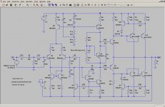
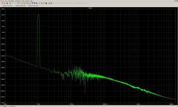
Here is a simulation of the VI limiter in action with a 0.001 ohm load.
The currents are within the limit for the MJL1302A/MJL3291A which is given as 15A continuous. BTW, the C suffixes in the circuit indicates that Cordell Audio's models were used, and is not part of the actual part number. The values for R20-23 can be changed for higher or lower limits. R26 also affects things.
The currents are within the limit for the MJL1302A/MJL3291A which is given as 15A continuous. BTW, the C suffixes in the circuit indicates that Cordell Audio's models were used, and is not part of the actual part number. The values for R20-23 can be changed for higher or lower limits. R26 also affects things.
Attachments
Last edited:
- Status
- This old topic is closed. If you want to reopen this topic, contact a moderator using the "Report Post" button.
- Home
- Amplifiers
- Solid State
- Engineer, help please - Neg. feedback/infilters