hey, I love the look of the amp, can you please post the schematic? because I think I am going to make an El34 PP design with PCBs, but I have no clue how to start making my own PCBs, not the manufacturing, I know loads about making the literal board, I just have no real clue how to start designing the board!
I think your amp looks amazing, and how much power do you get out of it?
I think your amp looks amazing, and how much power do you get out of it?
alexmoose said:hey, I love the look of the amp, can you please post the schematic? because I think I am going to make an El34 PP design with PCBs, but I have no clue how to start making my own PCBs, not the manufacturing, I know loads about making the literal board, I just have no real clue how to start designing the board!
I think your amp looks amazing, and how much power do you get out of it?
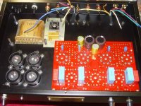
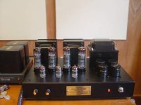
I am so sorry ,it was not my product¡£I just want to give some ideas to DIYers . its out about 30w in each channel.
tubes amps were required linking the ground wires at one point.so it not easy to make the pcbs. i advise u to draw the Circuit diagram on protel first(or u can get the classical diagram surf the internet ),then protel will make up it into pcb automatically. then u can adjust it by your will.
Most of us around here don't have and can't afford a legitimate copy of Protel - last time I checked a full/legal copy was about $6K. As a former Protel user and a current MentorGraphics DesignView user I can say none of these pro applications are particularly easy to use and have a steep learning curve.
I can recommend ExpressPCB, however you will have to create the tube symbols for your schematics (they explain how) and the octal and miniature tube sockets required. Once the schematic is complete you generate a netlist, link it to your pcb layout and go from there. If you post your artwork I can critique it, PM me and I can provide some fairly lousy socket symbols for the pcb layout side of things.
Incidentally auto-routing analog circuitry is considered a no-no, although most tube circuits are so simple that it probably isn't that hard to get it right if you know the basic rules.
Edit:
Get the software here: http://www.expresspcb.com/ Note I have no affiliation with this outfit, but do use their services regularly.
kevinkr said:
Incidentally auto-routing analog circuitry is considered a no-no, although most tube circuits are so simple that it probably isn't that hard to get it right if you know the basic rules.
what is auto-routing?
Auto-routing is a feature in high end pcb layout software that allows you to route all the traces automatically using a sets of rules about trace spacings, geometries and the like. It basically places the components and routes the connections between them automatically.
This can work pretty well in some digital application boards, however with faster speeds, critical timing between some signals, impedance considerations, noise and ground bounce problems it is not used in any critical design applications. We never use it on our ATE boards whether it is an actual instrument or test fixture board. Nothing like experience and a sharp human eye. Machine intelligence has come a long way but there still is no substitute for experience.
This can work pretty well in some digital application boards, however with faster speeds, critical timing between some signals, impedance considerations, noise and ground bounce problems it is not used in any critical design applications. We never use it on our ATE boards whether it is an actual instrument or test fixture board. Nothing like experience and a sharp human eye. Machine intelligence has come a long way but there still is no substitute for experience.
what is auto-routing?
In order to understand auto-routing, I must explain the PC board design process. It differs a bit depending on which PC board software that you are using. As Kevin explained some of the professional level programs are not user friendly, in fact some are user hostile. Eagle is a simple program that works well and a vacuum tube library is on their web site. The free version is only good for small boards though. I use the full blown (including auto router) version for all my boards.
I use Mentor Graphics in my full time job. It has impressive capabilities (my last board had 10 layers in HDI, and contained 1100 components on a 10 square inch board) that are totally unnecessary for vacuum tube work.
In the normal process of designing a PCB there are a few steps that are common between all of the different design software.
First you would input the desired schematic using a achematic editing package. Library symbols are required for each part. Common components like resistors are usually provided with the basic package. Unusual (to the rest of the engineering world) components like vacuum tubes are not supplied. They must be created by the user. Fortunately these symbols are often shared on the internet. Most library symbols also contain physical package information that is used in the PC board design process.
Next you import the schematic into the PC board layout program. Integrated packages like Eagle do this automatically.
If all went well there should be a graphical representation of all of your parts scattered randomly on a blank background. Each of your components should look like the actual physical components, and be scaled correctly.
Then you must draw (or import from a mechanical design program) the physical outline of the intended PC board. For our use it is often a simple rectangle. For something like a cellphone it will be a complex geometrical shape drawn in a mechanical engineering program like Pro Engineer. This is done to utilize every square millimeter of available board space.
The placement step comes next. This is where you should spend the most time. Here you will place all of the components onto the PC board in the position that it will occupy ot the final PC board. Here you must think ahead (like a Chess game) to visualize all of the connections that will be made to this component. There is a command in most programs to show the connections. (Ratsnest in Eagle). The connections appear as thin green or yellow lines. Try to organize the components to minimize the criss crossing of these lines. When the final board is done there is usually two sides available for running traces. You need to think about this as you are placing parts to avoid having traces running parallel to each other on opposite sides of the board unless it is intentional. After the parts are all placed on the board and you think they are in the correct places, you route the board.
Routing is the process of replacing the thin connection lines (called "guides" in Mentor, or "rats" in Eagle) with copper traces. In this process you will often find that a trace can not be routed due to another trace or a component in the way. This often requires ripping up a trace to route another one. This is an itterative process that can take considerable time. I will often have multiple copies of the same design with different routing strategies early in the design cycle, until I figure out which works the best. It is often necessary to go back and move some parts around to get an optimum route. Here again multiple copies is a good thing.
Auto-routing is the process of automating the routing process. You feed the auto router some information regarding your design rules, and preffered routing directions for each layer, and it will try to route your board automatically given your rules. This is often referred to as "rules based ripup and retry autorouting". The aurouter will not attempt to move any parts.
The autorouter available in any affordable program can be used to show you if a board is routable, and to find bottleneck areas. There no provisions for rules for noise, crosstalk, and other issues that are important to analog designers. I find that I can beat the autorouter in Eagle given enough time and patience. That means that Eagle will often give up and say that 2 or 3 traces can not be routed when I can route the board. I also find that the Eagle auto router can route a complex digital board when I can't. I would not use any affordable autorouter on a vacuum tube board. It can not tell if it just put the filament trace right next to the input trace.
On the other hand the Cadence auto router is very capable of doing these things given the proper "rules" in advance, and the 1100 part board would not have happened without it. Many autorouters will allow you to autoroute the digital section of a board, and complete the analog section by hand.
If the board was being made at a commercial PC board house, you would then generate "Gerber" files which are sent to them. For home fabrication the traces fro each side are often printed onto a transfer medium, or onto a transparancy for photographic transfer. You would then make a board and test it.
I see no mention of autorouting on their web site, but I have not used Express PCB. Keep in mind that Express PCB writes files in a proprietary format that is not accepted by most PC board houses. They give you the software because you have to buy the boards from them. I do not know if there is a method for using this software for making your own boards.
No, there is no auto-routing facility in ExpressPCB as the software is free-ware. However if you import the schematic netlist into the pcb it will highlight all points in a node that need to be connected together when you use the netlist tool.
And George is right, this is a software front-end for using the ExpressPCB service, if you wish to make your own boards you can use screen capture software to capture the different layers, then you will have to scale and print out plots. This actually isn't any worse than making pcbs from the artwork often found in older electronics magazines.
The manual file generation option in the program appears to be nothing more than another way to submit artwork to ExpressPCB - it doesn't seem to generate gerbers.
ExpressPCB is only inexpensive if you select the miniboard service which gives you three boards which are 3.8" x 2.5" two layer, with no silk screen, and no solder mask. Larger boards are available with standard service, protopro, and production, but are fairly expensive.
You would be surprised at what you can fit on one of these boards, I have managed to fit a 3 tube voltage regulator on one, clock regeneration on another, and most recently also used their miniboard service for a pair of boards I designed for my low noise mic pre-amplifier. (To measure Onken speaker system I designed and built a few months ago.)
An EL34 amplifier will not fit on one of these boards, but with careful design the driver stage will.
To maximize space I frequently use both sides of the board, use smd parts where possible and only use ground planes if really needed.
(mic amp/supply and a high speed ate app I did here at work.) 1206 SMD (1/4W) are not too hard to work with and are fine for most cathode, grid stoppers, and grid bias resistors. 2512 are larger still and will dissipate a 1/2W or more. I generally use through hole parts anywhere where high voltages are present.
Within the next few days I'll post a pix of my mic pre and power supply board, and the tube regulator so you can see what is possible.
Edit: fix formatting issues
- Status
- This old topic is closed. If you want to reopen this topic, contact a moderator using the "Report Post" button.
- Home
- Amplifiers
- Tubes / Valves
- EL34 make up by PCB