Trying to solve bias problems. The minimum quiescent current I can get is 520mA ....
When I play music at low levels, I need to set the quiescent current to 1.5A, when I play louder, it starts clicking, if i lower the current it goes away.
Really hard to explain what is going on. I think it is playing fully class B for higher volumes which results in cracking sound
When on low levels it's playinf full class A so it sounds okay, but hot transistors!
Last edited:
Another thing I noticed, one ballast resistor gets hot, while the other does not. I used IRF9540/640, they are not complementairy after all?
Have you checked the DC offset ? If that is out you will get more current through one output transistor.
Do you think that making a PCB for this amplifier would increase quality? Less noise?
I think I'm going to build a second one, to make this my first stereo amplifier.
This method is very cheap about €15/$21.
Making a PCB would cost me €50/$71.
Class AB is usually forgiving about layout unless you have gone silly with really long wires everywhere. I dont think you would gain much with a PCB except a nicer end product.
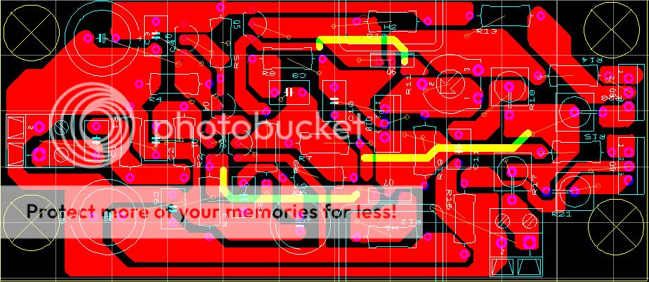
Heres a layout i made for a IRF540/9540 amp i built some months ago: http://i.imgur.com/mnk2q.png
Those boards are now running my lateral mosfet amp.
Those boards are now running my lateral mosfet amp.
Thank you for your design, I can't find your MJE350/340 or BD140/139 their symbols are small signal transistors. Also, there is no real input and output filtering. Where did you find the schematic?
Did you build it?
I actually have my own PCB lay-out, but it needs some modifications and I don't have the time right now, I'll post it in a few weeks.
edit: Oh, I just read your post after posting a comment. The only thing I'm concerned about is grounding. Right now I just made 1 starpoint, from there I go to the PSU.
Do long speakercables and cables from iPod,.. also cause oscillations? They also are part of the ground.
Last edited:
As long as theres good grounding within the amp, cables outside it shouldent affect it, however long speaker leads can make any amplifier unstable, but this is rarely any problem.
Why the drivers were small signal in my amp was that nothing more were needed, 2N5551 and 2N5401 were more than capable of driving the IRF540/954's.
Heres a vid of that amp playing: YouTube - Stereo mosfet amp
Why the drivers were small signal in my amp was that nothing more were needed, 2N5551 and 2N5401 were more than capable of driving the IRF540/954's.
Heres a vid of that amp playing: YouTube - Stereo mosfet amp
Class AB is usually forgiving about layout unless you have gone silly with really long wires everywhere. I dont think you would gain much with a PCB except a nicer end product.
Except when you're routing the feedback paths and connection nodes, and also high current tracks. Even a typical 'unconditionally stable' LIN amp can be made unstable with poor layout. It is certainly possible to properly layout a circuit like this, or even more complicated, onto vero-board but you want to stick to typical analog design rules.
") If you intend to build a high BW (~>200KHz) amplifer layout is critical even for class AB, otherwise you can swamp it with enough compensation that layout is less of a factor of operation.
If you intend to build a high BW (~>200KHz) amplifer layout is critical even for class AB, otherwise you can swamp it with enough compensation that layout is less of a factor of operation.
Vero board circuits may be more fragile and thus less reliable than etched or plated PCBs. When I vero board a circuit, I like to use solder to bridge the pads to create the tracks, then use jumper wires on the top side to essentially create a 2 layer PCB. It may use a lot of solder but I usually re-use it on another PCB when the circuit fails or is scraped for something better. BTW SMD components can be used in this manner as well. I use SOT-23 transistors and 0805, even 0603 resistors can be used with this method.
This is much more likely to happen without a Zobel filter and output coil to block RFI from the long speaker cables, or antena, from entering the feedback loop. I don't see an output coil on this amp........however long speaker leads can make any amplifier unstable, but this is rarely any problem.
 A simple suitable output coil for this amp can be made by taking a 10R 1/2W resistor and wraping 22Ga wire around it and soldering it to the leads of the resistor and repacing R17 with it. What the heck does R17 do anyway besides raise Zout of the amplifer?
Last edited:
I think you want the Vbe multiplier on the heatsink unless your using laterals, vertical fets will go into thermal runaway just like bipolars.
So i'd get it cadded in between the outputs or as a small separate board connecting by twisted wires to the main pcb like on my fetamp layout.
So i'd get it cadded in between the outputs or as a small separate board connecting by twisted wires to the main pcb like on my fetamp layout.
Like I said
The IRF510 for the VBE multiplier will be mounted on the heatsink with wires, output Fet's also I think.
I think you want the Vbe multiplier on the heatsink unless your using laterals, vertical fets will go into thermal runaway just like bipolars.
You can get away with the Vbe multiplier on the pcb if you use as low a bias as possible.
I found with my IRF240/9240 design I was managing to get as low as 7mA bias without crossover distortion. With that there was no need to mount the Vbe transistor on the heatsink.
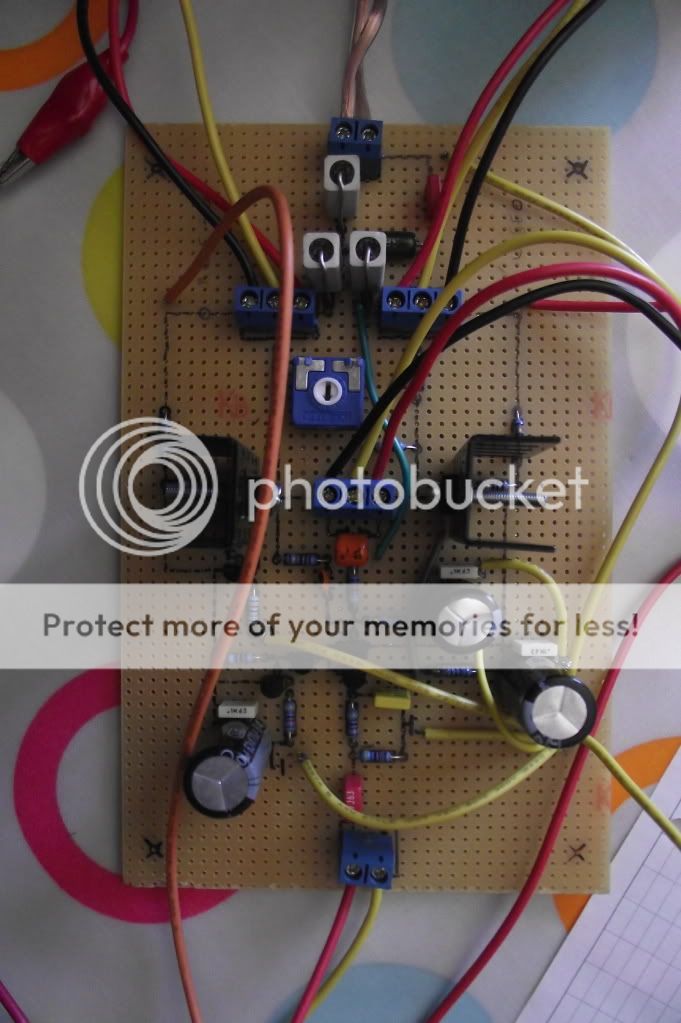
I am not able to use a scope right now. At the moment it is set like I like the sound. Fets does not heat up much. Barely feel a difference on the heatsink, it is 0,65K/W for both output Fets(on the same heatsink). The 'official' amp is going to use a 0,85K/W heatsink. I calculated that I need a heatsink of 1,07K/W for 50W at a efficiency of 33,3%.
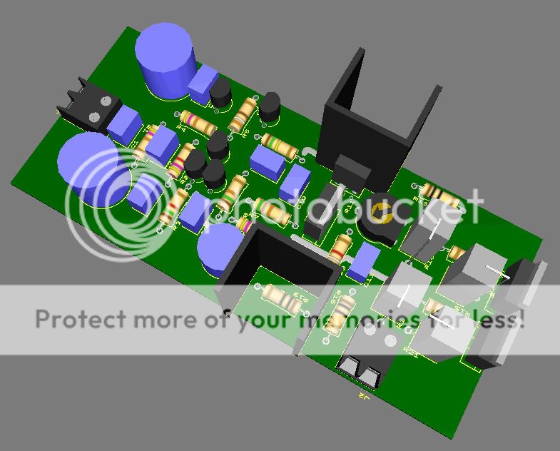
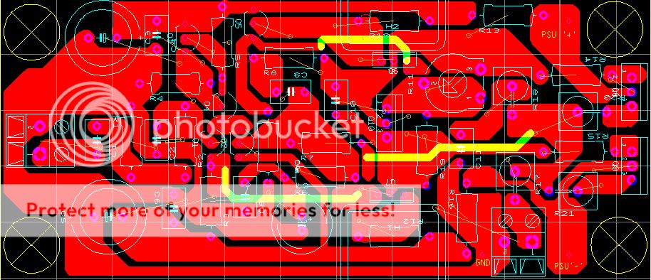
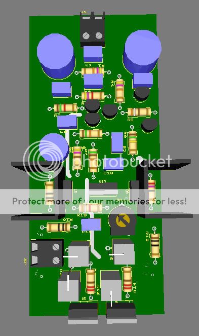
Are there any problems with my PCB lay-out?
Are there any problems with my PCB lay-out?
Last edited:
- Status
- This old topic is closed. If you want to reopen this topic, contact a moderator using the "Report Post" button.
- Home
- Amplifiers
- Solid State
- Easy and low cost: IRF540/9540 amp