That 36" length is just enough to wrap two turns around a 5.5" toroid.
That is very expensive !!!!!!
Guys, thank you for all your suggestions. Yesterday I made shield from double sided FR4 connected to GND and I haven't had any success. Picture follows later today.
Probably I will cut the PCB to reduce the size of it and place it in different casing. I just ordered toroid transformer with 4X12V output 50VA so that I can finally begin with some proper measurements.
BR,
Aleš
Probably I will cut the PCB to reduce the size of it and place it in different casing. I just ordered toroid transformer with 4X12V output 50VA so that I can finally begin with some proper measurements.
BR,
Aleš
i could be wrong here but looking at your boards it looks like you have not linked the secondary's together, marked with yellow lines in picture below.
looking at the transformers they indicate 0-12 + 0-12 which to me says that they are 2x12v output. only problem is if you do link them you will have 24v. if you haven't/dont link them where are the other ends of the windings going?
or are you using the 'centres' as a GND in which case you have an AC ground plane instead of DC.
single 2x12v transformer
An externally hosted image should be here but it was not working when we last tested it.
Last edited:
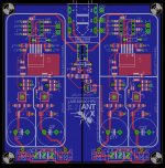
Ok so version with transformers on the PCB has flaws therefore I decided to go for version without them. During the PCB build I noticed some errors and a lot of improvement for components placing.
On the PCB is now jack connector instead of ALPS RK27 as someone might want to use something different/better. Connector is NMJ6FHD2 and next to it there are pads so this amplifier can also be used as preamplifier, while testing current version I was quite amazed how good it sounds. Input pads are now closer to each channel.
Power supply is also redisigned. On the AC input are now schottky diodes (easier manufacturing and lower voltage drop). After them are pads for DC input if more capacitance filtering is desired. Filtering capacitors are now 18mm dia, so Panasonic 5600uF 25V can now fit. Positive regulators are TPS7A4700 instead of 4701, preset at 12V. On all output lines there is now place for ferrite bead, so sound can become more relaxed and not so fast, though easily shorted if one will find them not useful. Over output capacitors next to the regulators I made vias so sound character can be changed with different elcos, such as Elna nichicon etc.. Components around VAS stage are now more closely to the operational amplifier.
Best Regards,
Aleš
Attachments
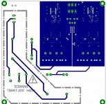
i could be wrong but i dont think you can do that for a GND. what you have done is tied all the secondary's together (flow and return) and also tied the two transformers together which i'm sure is not a good idea. this has given you an AC GND rather than a DC GND, i also think that bridging the 2 secondary doubles the voltage to 24v but i could be wrong on all counts.
also regarding anodised cases, you need to scrape a little bit of the anodising off all mating faces or you end up with just one panel being earthed.
also regarding anodised cases, you need to scrape a little bit of the anodising off all mating faces or you end up with just one panel being earthed.
Hi Aleš,
I've been following some of your threads on this forum and was greatly inspired by your TPS4700 PSU design while working on my own TPS30/TPS49 symmetric PSU.
I must say I am not an expert, but looking at your layout some thing could probably be further improved, IMHO. I would suggest to change the order of C1<->C2 and C3<->C4 -> smaller cap closer to the IC pins... Also power lines to LME49600 could be made symmetric if the heat sink pad is made symmetric with respect to the IC. This will allow better use of C3, C4 caps which are now past the chip pins if looking from the PSU so decoupling could be better if the power supply trace would first touch the C3 then C4 and then the chip power pins. Heat sink tab does not have to be used as power supply conductor, IMHO.
You could also "beautify" the layout further if you move the ICs U1/U3 a bit to the left and U2/U4 a bit to the right which will let you to align power traces from the big filter capacitors pins. Also, C10 can be aligned with the C30 to make smaller footprint for the delay circuit... same with the transistor+C20 combo which can be turned 90 degree clockwise and shifted a bit to the left... It will make near symmetric layout for the delay network. The output connector can be placed symmetrically between the relay and the headphone connector with two GND pads in the middle in case someone decide to make a custom dual mono headphones cable... To accomplish this you could extend the GND plane cut in the middle all the way to the edge of the board. This way if the headphone connector is not soldered to the board the GNDs of both left and right channels are separated making it real dual mono. You can make SMD solder bridge for the left and right channel GNDs under the headphone connector if someone needs to connect them.
Just my two cent...
Regards,
Oleg
i could be wrong but i dont think you can do that for a GND. what you have done is tied all the secondary's together (flow and return) and also tied the two transformers together which i'm sure is not a good idea. this has given you an AC GND rather than a DC GND, i also think that bridging the 2 secondary doubles the voltage to 24v but i could be wrong on all counts.
...Removed transformers from PCB and used 15cm long wires to connect them back. Now I have no hum. I also experimented which transformer is producing this noise and it appears to be the one next to the switch, interfering with left channel...
Of course it doubles the voltage because I have connected two windings together. But when measured to the center tap you get rated voltage. So what I did is basically center tapped transformer out of transformer with dual secondaries.
also regarding anodised cases, you need to scrape a little bit of the anodising off all mating faces or you end up with just one panel being earthed.
I agree with you, but you can be sure that I checked if the whole casing was grounded and that earth wire from IEC inlet has contact to the back panel.
BR,
Aleš
Hi Aleš,
I've been following some of your threads on this forum and was greatly inspired by your TPS4700 PSU design while working on my own TPS30/TPS49 symmetric PSU.
I must say I am not an expert, but looking at your layout some thing could probably be further improved, IMHO. I would suggest to change the order of C1<->C2 and C3<->C4 -> smaller cap closer to the IC pins... Also power lines to LME49600 could be made symmetric if the heat sink pad is made symmetric with respect to the IC. This will allow better use of C3, C4 caps which are now past the chip pins if looking from the PSU so decoupling could be better if the power supply trace would first touch the C3 then C4 and then the chip power pins. Heat sink tab does not have to be used as power supply conductor, IMHO.
You could also "beautify" the layout further if you move the ICs U1/U3 a bit to the left and U2/U4 a bit to the right which will let you to align power traces from the big filter capacitors pins. Also, C10 can be aligned with the C30 to make smaller footprint for the delay circuit... same with the transistor+C20 combo which can be turned 90 degree clockwise and shifted a bit to the left... It will make near symmetric layout for the delay network. The output connector can be placed symmetrically between the relay and the headphone connector with two GND pads in the middle in case someone decide to make a custom dual mono headphones cable... To accomplish this you could extend the GND plane cut in the middle all the way to the edge of the board. This way if the headphone connector is not soldered to the board the GNDs of both left and right channels are separated making it real dual mono. You can make SMD solder bridge for the left and right channel GNDs under the headphone connector if someone needs to connect them.
Just my two cent...
Regards,
Oleg
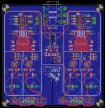
Oleg thank you for your suggestions. I used some of them as much as I could. I especially liked the idea to make symmetry for the power lines and to swap C1 C2 and C3 C4 capacitors. Never really gave much thought about it.
Attachments
Looks good!
A couple of concerns On your boards U1/U3 are TPS7A4700 while U2/U4 are TPS7A4701 if I am not mistaken... Also, you have reduced heat sink area a bit for the LME49600s. I do not see a reason to do it, you can make heat sink area bigger if you wish, you have a lot of empty space on your PCBs.
Regards,
Oleg
A couple of concerns
On your boards U1/U3 are TPS7A4700 while U2/U4 are TPS7A4701 if I am not mistaken... Also, you have reduced heat sink area a bit for the LME49600s. I do not see a reason to do it, you can make heat sink area bigger if you wish, you have a lot of empty space on your PCBs. Regards,
Oleg
Yeah I went for TPS7A4700 because on current version I had some voltage difference between + and - rail, even though I used resistors with 0.5% accurancy. With TPS7A4700 I expect to have some difference also, but at a gain that now are 6 parts less on the PCB.
LME49600 didn't produce much heat during testing of current version, about 5°C more than ambient temperature, so smaller heatsink area isn't much of concern. Still I left enough area around it to mount TO-263 heatsink.
Best Regards,
Aleš
LME49600 didn't produce much heat during testing of current version, about 5°C more than ambient temperature, so smaller heatsink area isn't much of concern. Still I left enough area around it to mount TO-263 heatsink.
Best Regards,
Aleš
Great board. I suppose it's not possible to add a SOIC-8 footprint for the opamp?
Well I could but then some tracks would be longer. Still SOIC to DIP adapter can be used.
So today I received new transformer, this time toroid one. Its specs are 4 x 12V, 50VA, with magnetic shield and encapsulated into plastic casing. Where ever I place it around PCB I don't have any 50Hz hum or any other noise
. BR,
Aleš
Great news, Aleš!
Usually toroid transformers have a different magnetic field, this is why are so largely used for Hi-Fi equipment with small cases. Anyway, if the case is too thick, then when you'll close the case some hum might be audible, even with toroid inside, because magnetic fields will close through the case and spread around for 2-3 inches. So, you may want to test for the hum after finding an enclosure, just in case...
Thank you,
Raul.
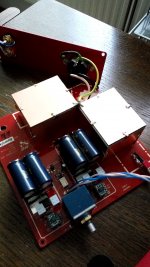
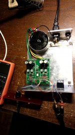
Prototype No. 2
So here it is prototype no. 2. It works like a charm, but building it is really a night mare comparing to the prototype no. 1, if you ask me. To properly wire potentiometer and to avoid hum I really needed to put much more effort into build, where in previous version I just inserted pot into PCB, soldered it and job was done. The other thing with pot off PCB is that if one of the output wires from it (from pot) gets loose or something, opamp input is floating and has no reference to ground. DC servo can't do its job and output DC voltage can be as high as 10V, ouch . 220pF capacitor from input to ground solves this problem easily.
After all these flaws I made, I started to look other other headphone amps, diy and manufactured ones, how those are build. On almost all of them potentiometer is on the PCB. This simplifies production and hum is much more easily avoided.
I think I'll be lucky with prototype No. 3
BTW the sound from No.2 has much more micro details and 3D imaging comparing to No.1.
Best Regards,
Aleš
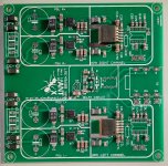
Photo of PCB

Photo of prototype

So here it is prototype no. 2. It works like a charm, but building it is really a night mare comparing to the prototype no. 1, if you ask me. To properly wire potentiometer and to avoid hum I really needed to put much more effort into build, where in previous version I just inserted pot into PCB, soldered it and job was done. The other thing with pot off PCB is that if one of the output wires from it (from pot) gets loose or something, opamp input is floating and has no reference to ground. DC servo can't do its job and output DC voltage can be as high as 10V, ouch
. 220pF capacitor from input to ground solves this problem easily. After all these flaws I made, I started to look other other headphone amps, diy and manufactured ones, how those are build. On almost all of them potentiometer is on the PCB. This simplifies production and hum is much more easily avoided.
I think I'll be lucky with prototype No. 3
BTW the sound from No.2 has much more micro details and 3D imaging comparing to No.1.
Best Regards,
Aleš
Photo of PCB
Photo of prototype
A couple of observations.
Your design is sensitive to magnetics because you have inductors in your feedback
loop for your regulators. I'm surprised it doesn't oscillate.
Your delay relay should short the output when not energized.
That way, when it is energized, it removes itself from the circuit.
Your design is sensitive to magnetics because you have inductors in your feedback
loop for your regulators. I'm surprised it doesn't oscillate.
Your delay relay should short the output when not energized.
That way, when it is energized, it removes itself from the circuit.
- Status
- This old topic is closed. If you want to reopen this topic, contact a moderator using the "Report Post" button.
- Home
- Amplifiers
- Headphone Systems
- Dual mono LME49600