The IRF540 has listed four times for switching. Add those and you will find out the dead time needed.
If you added dead time, maybe that is what you are seeing. That step will be there no matter what. It is just better to be there because both transistors are OFF (as oposed to being ON simultaneous).
Class AB does not apply here - you don't have any negative feedback involved. It's just class D.
If you added dead time, maybe that is what you are seeing. That step will be there no matter what. It is just better to be there because both transistors are OFF (as oposed to being ON simultaneous).
Class AB does not apply here - you don't have any negative feedback involved. It's just class D.
IRF540, if I make 2nd version I will change from IRF24.
implemented Dead-time control code is here.
when
DSD L to H
High Side 0 0 0 0 1 1 1 1
Low Side 1 1 1 0 0 0 0 0
DSD H to L
High Side 1 1 1 1 0 0 0 0
Low Side 0 0 0 0 0 1 1 1
AB amplification and negative feed back is different issue.
(the issue for 1 stage of transistor, how works)
implemented Dead-time control code is here.
when
DSD L to H
High Side 0 0 0 0 1 1 1 1
Low Side 1 1 1 0 0 0 0 0
DSD H to L
High Side 1 1 1 1 0 0 0 0
Low Side 0 0 0 0 0 1 1 1
Code:
	DSD_OUT_1: process(MCLK, DSD_4, CH01, FIFO_EFN, RESETN)
	begin
		-- output SD signal from I2S side registers. parallel to serial, just long and wide
		if RESETN = '0' or FIFO_EFN = '0' then
			DSDL_P <= '0';
			DSDL_N <= '0';
			DSDR_P <= '0';
			DSDR_N <= '0';
		elsif MCLK' event and MCLK = '1' then
			case DSD_4 is
				when B"00" => null;
				when B"01" => null;
				when B"10" => null;
				when B"11" =>
					DSDL_P <= CH01(0);
					DSDL_N <= not CH01(0);
					DSDR_P <= CH01(1);
					DSDR_N <= not CH01(1);
				when others => null;
			end case;
		end if;
	end process;

	--Dead Time Control
	Deadtime_Signal: process(FPGA_CLK, RESETN, DSDL_P, DSDL_N, DSDR_P, DSDR_N)
	begin
		if RESETN = '0' then
			DSDL_P_1 <= '0';
			DSDL_N_1 <= '0';
			DSDR_P_1 <= '0';
			DSDR_N_1 <= '0';
			DSDL_P_2 <= '0';
			DSDL_N_2 <= '0';
			DSDR_P_2 <= '0';
			DSDR_N_2 <= '0';
			DSDL_P_3 <= '0';
			DSDL_N_3 <= '0';
			DSDR_P_3 <= '0';
			DSDR_N_3 <= '0';
			DSDL_P_4 <= '0';
			DSDL_N_4 <= '0';
			DSDR_P_4 <= '0';
			DSDR_N_4 <= '0';
		elsif FPGA_CLK' event and FPGA_CLK = '1' then
			DSDL_P_1 <= DSDL_P;
			DSDL_N_1 <= DSDL_N;
			DSDR_P_1 <= DSDR_P;
			DSDR_N_1 <= DSDR_N;
			DSDL_P_2 <= DSDL_P_1;
			DSDL_N_2 <= DSDL_N_1;
			DSDR_P_2 <= DSDR_P_1;
			DSDR_N_2 <= DSDR_N_1;
			DSDL_P_3 <= DSDL_P_2;
			DSDL_N_3 <= DSDL_N_2;
			DSDR_P_3 <= DSDR_P_2;
			DSDR_N_3 <= DSDR_N_2;
			DSDL_P_4 <= DSDL_P_3;
			DSDL_N_4 <= DSDL_N_3;
			DSDR_P_4 <= DSDR_P_3;
			DSDR_N_4 <= DSDR_N_3;
		else
			null;
		end if;
	end process;

	--make actual output, dead-time controlled
	--TC4428, pin2 - #OUTA - H is Off, Low  side.
	--        pin4 -  OUTB - H is ON,  High side.
	DeadTimed_Output_L_P : process(DSDL_P_1, DSDL_P_2, DSDL_P_3, DSDL_P_4)
	begin
		DSDL_OUTPH <= DSDL_P_2 and DSDL_P_3;
		DSDL_OUTPL <= DSDL_P_1 or DSDL_P_2 or DSDL_P_3 or DSDL_P_4;
	end process;
	DeadTimed_Output_L_N : process(DSDL_N_1, DSDL_N_2, DSDL_N_3, DSDL_N_4)
	begin
		DSDL_OUTNH <= DSDL_N_2 and DSDL_N_3;
		DSDL_OUTNL <= DSDL_N_1 or DSDL_N_2 or DSDL_N_3 or DSDL_N_4;
	end process;
	DeadTimed_Output_R_P : process(DSDR_P_1, DSDR_P_2, DSDR_P_3, DSDR_P_4)
	begin
		DSDR_OUTPH <= DSDR_P_2 and DSDR_P_3;
		DSDR_OUTPL <= DSDR_P_1 or DSDR_P_2 or DSDR_P_3 or DSDR_P_4;
	end process;
	DeadTimed_Output_R_N : process(DSDR_N_1, DSDR_N_2, DSDR_N_3, DSDR_N_4)
	begin
		DSDR_OUTNH <= DSDR_N_2 and DSDR_N_3;
		DSDR_OUTNL <= DSDR_N_1 or DSDR_N_2 or DSDR_N_3 or DSDR_N_4;
	end process;
AB amplification and negative feed back is different issue.
(the issue for 1 stage of transistor, how works)
Last edited:
You are a prolific programmer ")
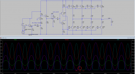
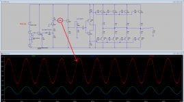
You mean IRF240? That's kind of slow (total of 297ns delay compared with 120ns for IRF540).
PS: I know that AB is a different issue than negative feedback, but it does not make sense one without other. Class D does not require analog bias or feedback.
Although, a curent feedback can compensate for load's variable impedance...
Last edited:
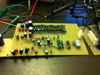
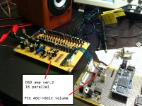
16 parallel is working. I'm listening single channel, but sounds like magic, natural.
I'm using AudioPro Bravo FX-01 now, but I feel want to try MarkAudio full range with DSD direct amp.
1kHz THD: 0.15%, It looks like this is an amplifier of good birth.
The most fun is now only I am listening this sound, pure DSD signal just before LPF.. then suddenly the music appears on the speaker terminal.
and components are, 74HC08, 2N3904/3906, caps, resistors. in 21 century
The reason of distortion and noise, I remember 2nd stage (Base Common) is high-speed, but has 0dB PSRR. (PSU_Noise.png) omg.
So current usage of final stage may return to here.
This stage must be separated from other stages. Others are Emitter follower, have very high PSRR.
By this experiment,
(a) Volume can be controlled by pulse height (DSD + parallel -> AND gate -> R-2R).
(b) paralleled small Tr can amplify > 10MHz signal, and very clean. By LTSpice, -3dB point is 42MHz.
Next version...
(1) 64? parallel
(2) DC offset controller (I added pot, annoying)
(3) Clean supply for base common amp
(4) I need PCB, too hard to solder.
I forgot how to make analog amp
Now I'm watching how to handle DSD signal from source to amp output.
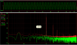
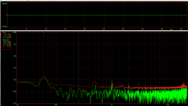
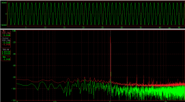
NoConnect.png: nothing connected, Cheap Behringer UCA202 shows -90dB noise floor.
FPGA_Direct.png: DSD_L output-> RC LPF -> level control ->UCA202.
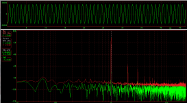
Buffered.png: DSD_L output-> 74HC244 Buffer -> RC LPF -> level control ->UCA202.
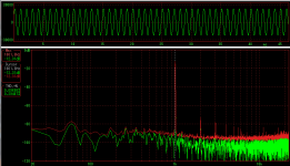
Reclocked.png: DSD_L output-> 74HC574 FF -> RC LPF -> level control ->UCA202.
So, DSD signal should be handled by Fast logic, not to be buffered or reclocked by slow gates.
modification for 1/0 pulse curve / width = non linear distortion.
not only amplification, but signal path must be fast / symmetric for positive - negative slew rate.
Now I'm watching how to handle DSD signal from source to amp output.
NoConnect.png: nothing connected, Cheap Behringer UCA202 shows -90dB noise floor.
FPGA_Direct.png: DSD_L output-> RC LPF -> level control ->UCA202.
Buffered.png: DSD_L output-> 74HC244 Buffer -> RC LPF -> level control ->UCA202.
Reclocked.png: DSD_L output-> 74HC574 FF -> RC LPF -> level control ->UCA202.
So, DSD signal should be handled by Fast logic, not to be buffered or reclocked by slow gates.
modification for 1/0 pulse curve / width = non linear distortion.
not only amplification, but signal path must be fast / symmetric for positive - negative slew rate.
Attachments
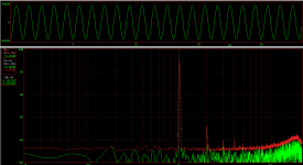
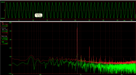
I received 74AC08/32/74/244 yesterday and tested DSD quality.
not better than FPGA output... Xilinx is faster than 74AC.
74AC's t(L->H) = 4 to 16 ns, (around 8ns on oscillo), t(H->L) = 3.5 to 14ns (around 6ns on oscillo)
Maybe I need NC7SV08/32 etc (very fast, 1ns/3.3V) device to get "better than FPGA" result.
WaveForm shows only a slight difference, but 2ns difference is very large for DSD signal. Pulse width difference 1% makes 1% 0 cross point distortion.
DAC chip handles reclocking and conversion in one chip, but I want to make direct DSD amp on PCB board. difficult..
Attachments
Hi Koon,
Great work!
I have been playing with dsd signal and FT232H a year ago, buy in opposite way: to grab DSD data into PC from SACD player.
There are several thoughts, I hope they will be helpful for you:
1. Working around dead-time with this way:
2. I would consider a slightly easier approach: to prepare all needed data in software and deliver them with FT232H using async 245 mode. In that way 4 data lines needed for each channel in bridged arrangement:
3. I have read some articles on inductorless Class-D amps and think that it should work for DSD-amp. If one side of the bridged amp is fed with 1 tick delay, it should remove HF signal. Do you have any ideas on this?
Great work!
I have been playing with dsd signal and FT232H a year ago, buy in opposite way: to grab DSD data into PC from SACD player.
There are several thoughts, I hope they will be helpful for you:
1. Working around dead-time with this way:
looks not great for me. First, you will always get more "1" on top than on bottom, and second, common-mode signal is not constant anymore. Have you seen this doc http://www.grimmaudio.com/whitepapers/discrete%20ad%20converter.pdf? It contains some notes on how to rearrange top and bottom bits a little better.DSD L to H
High Side 0 0 0 0 1 1 1 1
Low Side 1 1 1 0 0 0 0 0
DSD H to L
High Side 1 1 1 1 0 0 0 0
Low Side 0 0 0 0 0 1 1 1
2. I would consider a slightly easier approach: to prepare all needed data in software and deliver them with FT232H using async 245 mode. In that way 4 data lines needed for each channel in bridged arrangement:
PDATA+
PDATA-
NDATA+
NDATA-
but no signal processing is needed on the amp side. Also, no FIFO buffer will be needed, FT232H output buffer will do the job. PDATA-
NDATA+
NDATA-
3. I have read some articles on inductorless Class-D amps and think that it should work for DSD-amp. If one side of the bridged amp is fed with 1 tick delay, it should remove HF signal. Do you have any ideas on this?
Hi Kiwi, Now I'm free from dead-time issue.
Here is "straight DSD amplifier".
(1) DSD pulse height control volume: parallel ADC + AND gates + R-2R DAC
(2) High speed pre amplifier, 2N3904/3906 (+-15V, regulated)
(3) 16 parallel driver amp, 2N5550/5401 (+-17V)
Now I'm listening single channel, have to solder one more board
Here is "straight DSD amplifier".
(1) DSD pulse height control volume: parallel ADC + AND gates + R-2R DAC
(2) High speed pre amplifier, 2N3904/3906 (+-15V, regulated)
(3) 16 parallel driver amp, 2N5550/5401 (+-17V)
Now I'm listening single channel, have to solder one more board
Attachments
(1) DSD pulse height control volume: parallel ADC + AND gates + R-2R DAC
That is an interesting aproach - hybrid final stage (digital/analog). I am very interested in this, maybe you can post some measurements. I know it is hard without a proper distortion meter - with just the ADC's in our sound cards...
Hi Bunpei san
This circuit has no clock, so can accept 5.6MHz.
The amplifier bandwidth, LTSpice says -3dB @ 28MHz.
Hi Sonic,
Waveform: I can watch DSD pulse height changes as I thought.
Distortion: I have UCA202 (16bit) ADC but now insufficient to measure..
Still I'm watching waveforms, please wait for finalized. or Please reproduce on your desk and help
I thought again and I am cofused why you need the analog attenuation in the final stage. I thought that your DSP will take care of the volume control in the PCM stage and keep the finals in pure comutation mode only?
The way it is now, the finals will not be saturated and they will overheat. It is no better than using a LF filter before an analog amplifier.
Or even better use the inside of a modern DAC - two HF-capable curent sources, one charging a capacitor and the other discharging it, to make the analog out.
Hi Sonic
Pulse Height | DSP control: DSP volume control is impossible for DSD signal. There are no PCM stage.
Class D stage: no power loss but there is switching. I don't want to think about deadtime issue.
Analog Stage: consumes idle current, total 80mA. I don't care this power loss, eliminating dead-time control. DSD signal goes as it is.
LPF(DSD-DAC) then amplify | straight DSD amplification then LPF: one DSD pulse will remain around some msecs, by LPF post echo. so, DSD then LPF means thousands of pulse amplification are summarized to audio signal.
in other word.. amplify then LPF = amplify 10Hz to 2.8MHz then take only 10Hz to 30kHz.
amplification error is reduced (30000/2800000).
- Status
- This old topic is closed. If you want to reopen this topic, contact a moderator using the "Report Post" button.
- Home
- Source & Line
- Digital Source
- DSD Playback system, DSF Player + USB DDC + DSD Amplifier