It is welcome that you are testing this latest and simple version.
Have you been able to verify the shift in DC at the output with the temperature? The two diodes 1N4148 do their job?
What idle current have you measured? If this current is excessive (such as above 2 A), you can increase the resistor associated with the 1K trimpot. You would have to adjust the offset again.
I look forward to the results of distortion measurements.
Best regards
I have around 1,3A current, the supply is abt +-13V. I did not read all of the thread, should the diodes be mounted on the heat sink?
I still have some 'adjustments' to do, I'm thinking some decoupling capacitors close to the fet's would be good.
Thank you for your work with this design!
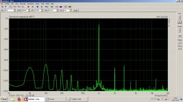
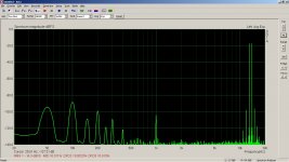
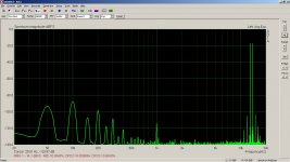
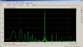
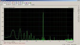
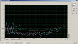
DLH distortion measurements
So, here are some measurements. I was not able to drive it harder than 8Vpp, due to limitation on the sound card output (get some distortion at max output), and low gain in the amp.
My basic measurement setup picks up quite a lot of noise, a lot from the 50Hz mains, something around 12kHz, and higher too, so please do not look to much into these areas. It also affects the THD calculation (in a negative way) seen at the bottom of the screen.
The 1k pot has been adjusted to give the lowest distortion. The optimal adjustment seems to differ between 4 & 8 ohms. Transistors are not matched. Capacitors are 'quality' capacitors, and resistors are metal film. The 'layout' might have some influence on the results too..
Power supply is linear CRC with 5x6800uF and 0,08ohm per rail. Wires to the amp board are a bit thin at 0,5mm2..
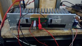
Filenames for the pictures explain the measurement condition (the picture of the board is before I added the gate resistors).
So, here are some measurements. I was not able to drive it harder than 8Vpp, due to limitation on the sound card output (get some distortion at max output), and low gain in the amp.
My basic measurement setup picks up quite a lot of noise, a lot from the 50Hz mains, something around 12kHz, and higher too, so please do not look to much into these areas. It also affects the THD calculation (in a negative way) seen at the bottom of the screen.
The 1k pot has been adjusted to give the lowest distortion. The optimal adjustment seems to differ between 4 & 8 ohms. Transistors are not matched. Capacitors are 'quality' capacitors, and resistors are metal film. The 'layout' might have some influence on the results too..
Power supply is linear CRC with 5x6800uF and 0,08ohm per rail. Wires to the amp board are a bit thin at 0,5mm2..
Filenames for the pictures explain the measurement condition (the picture of the board is before I added the gate resistors).
Attachments
Last edited:
Truly surprised by the outstanding measurement results. I am very pleased to know that it is a variant with a very low IMD.
According to the settings I see, it should be very pleasant to hear the range between 70 Hz and 2 KHz, with a high range above 2 KHz quite detailed.
I believe that the diodes would do their job better by staying close to the bipolar transistors of the input circuit. It would be interesting if you measure if there are significant DC shifts at the output, after stabilizing a certain final operating temperature.
I think it is an amplifier that shows two very different faces: on the one hand, its extreme simplicity may not be attractive to those who are accustomed to expecting good results from more complex circuits; On the other hand, its outstanding performance seems unable to be associated with its extreme simplicity, surprising more than one experienced builder.
Best regards
According to the settings I see, it should be very pleasant to hear the range between 70 Hz and 2 KHz, with a high range above 2 KHz quite detailed.
I believe that the diodes would do their job better by staying close to the bipolar transistors of the input circuit. It would be interesting if you measure if there are significant DC shifts at the output, after stabilizing a certain final operating temperature.
I think it is an amplifier that shows two very different faces: on the one hand, its extreme simplicity may not be attractive to those who are accustomed to expecting good results from more complex circuits; On the other hand, its outstanding performance seems unable to be associated with its extreme simplicity, surprising more than one experienced builder
.Best regards
Bad news
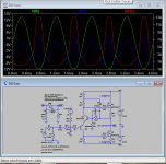
Unfortunately, this circuit has a critical flaw as demonstrated by simulating it at clipping while viewing the FET current. At the somewhat premature negative clipping, both FETs become turned on resulting in a huge shoot through current.
I thought there might be a easy fix by adding an offset to the upper FET drive but that just results in premature positive clipping, albeit without shoot-through current. I also tried to move the BJT emitter voltage but nothing seems to help without alternate problems. The more I try to make this work, the more I think that circuits like it were abandoned years ago for good reason.
Attachments
Well, I guess with it having the benefit of being a simple circuit, it has it's drawbacks too.
Maybe adding some limiter on the input preventing clipping would be an effective workaround to keep it simple? Maybe you can simulate a limiter circuit for it? Would be nice to get it with some different 'settings' depending on supply voltage.
Measurement performance seems good enough for the circuit as it is.
I see you have source resistors on the simulated circuit, probably limiting the shoot through current, wonder how it looks with the one I built without resistors?
I'm a bit curious about PSRR on this circuit?
Diego: Ok, the diodes are next to the 560 transistor, but not 'thermally connected'. I remember the offset changing while I was testing. I adjusted it one more time after testing when it was stable in temp, so I could just turn it on and double check when it's warm again today.
Last edited:
When I turned it on cold, offset was abt +0,5V, and current abt 0,7A, after abt 10min it had reached abt +0,1V and current just over 1A. After more than one hour, I see -0,2V and 1,65A, so I adjusted the offset to near 0 again, and current also went down to abt 1,5A. It seems to be moving around a bit in current and offset depending on temperature.
EDIT: Now it's sudddenly down to 1A and a little positive on offset again. Not very stable it seems..
EDIT: Now it's sudddenly down to 1A and a little positive on offset again. Not very stable it seems..
Last edited:
Unfortunately, this circuit has a critical flaw as demonstrated by simulating it at clipping while viewing the FET current. At the somewhat premature negative clipping, both FETs become turned on resulting in a huge shoot through current.
I thought there might be a easy fix by adding an offset to the upper FET drive but that just results in premature positive clipping, albeit without shoot-through current. I also tried to move the BJT emitter voltage but nothing seems to help without alternate problems. The more I try to make this work, the more I think that circuits like it were abandoned years ago for good reason.
I have never set out as a design objective for the DLH that more than 2 VRMS are injected into its input. According to what is observed in its simulation, the input signal would be close to 3.5 VRMS, almost 77% more than the original value of design. In addition, some values and components have been visibly modified. The generality of the conclusions would not apply here.
Please analyze the circuit as it was presented in its different variants. It is obvious that they all have limitations and that there will be cuts in the negative half-wave of the output signal, if the design limits are exceeded.
Best regards
When I turned it on cold, offset was abt +0,5V, and current abt 0,7A, after abt 10min it had reached abt +0,1V and current just over 1A. After more than one hour, I see -0,2V and 1,65A, so I adjusted the offset to near 0 again, and current also went down to abt 1,5A. It seems to be moving around a bit in current and offset depending on temperature.
EDIT: Now it's sudddenly down to 1A and a little positive on offset again. Not very stable it seems..
Adjusting the DC offset and idle current take several progressive cycles. It is a rather tedious task, until reaching the desired point.
It is similar to the case of the JLH using a split power supply and without an output capacitor.
For the stabilization time of the final parameters, it may be helpful to reduce the value of the input capacitor from 220 uF to a minimum such as 1 uF, without too much detriment to the low frequencies.
Best regards
What changes need to be made to the circuit when using power supply + - 18 V?
DLH Amplifier-Trilogy with PLH and JLH Amplifiers - Share Project - PCBWay
DLH Amplifier-Trilogy with PLH and JLH Amplifiers - Share Project - PCBWay
Diego,
This struck me from SteveEU:
He is correct. Perhaps best to use the Rush Cascode only as an input stage, affording non-inverting and inverting nodes with differential action a la LTP, and use it to drive a VAS in the conventional Self Blameless. This could the best option, delivering speed, low phase shift and avoid the negative clip issue.
Hugh
This struck me from SteveEU:
Unfortunately, this circuit has a critical flaw as demonstrated by simulating it at clipping while viewing the FET current.
He is correct. Perhaps best to use the Rush Cascode only as an input stage, affording non-inverting and inverting nodes with differential action a la LTP, and use it to drive a VAS in the conventional Self Blameless. This could the best option, delivering speed, low phase shift and avoid the negative clip issue.
Hugh
I stated the problem in #363 and now Steve has to rediscover it all over again.This struck me from SteveEU:
He is correct. ...
But Diego prefers to leave those who builds DLH in the viper pit. You can see his response :...I also found inherent destructive cross conduction problem for input signals larger than 3V in my simulation. I suggest some kind of input over voltage protection.
Please edit and state these limitations on post #1 before too many people use other supply voltage or large input signal that will destroy the output mosfets and kill the speakers.
I found this issue as negligence of the OP. There is no shame in preventing disastrous usage from builders. Even big names like Hiraga published a schematic with similar issue in the past. Builders beware!!!... I make this clarification again: the DLH was developed as it was presented bearing in mind as many quality premises as possible. The input signal that was anticipated was the one that can deliver the output of a typical CD player (2 V RMS).
Whoever needs to adapt it to build it with other values of available elements, can do it perfectly, but will have to recalculate it without losing quality as its main objective. It is not impossible, but whoever has to do it will have to resort to his own abilities....
Last edited:
I do not understand the reasons for discrediting a particular design, by pretending that the same design continues to behave well even outside its original specifications.
I have already said it and I repeat it again: whoever wants the DLH to admit thousands of volts as an input signal, to redesign it and adjust it at his own effort and risk.
I can only circumscribe the operation of what I have shared and designed, within the limits of use clearly informed.
On the other hand, as the efficiency of consumption has not been an objective in the design of the DLH, an asymmetric clipping is not a concern, if it is used within the given limits (giving sufficiently safe margins of operation outside any signal cut-off) .
I do not believe that neither Pass, nor Hood, nor Hiraga, have shared designs so that they are used well outside of their design objectives.
Possibly, whoever claims otherwise, has not even built the DLH to discuss with good intention and constructive contribution.
Best regards
No, your design is good and produce beautiful music, it only needs safety protection for reasonable usage.
I can not understand why you are against an addition of a simple clamp to limit input within the safe 2VRMS level. Back to back parallel of 4 silicon diodes like 1N4148 in series should do it as a simple solution to protect against mishaps like source voltage being too high and static electricity, catastrophic to both speakers and amp. Show us a design from Pass, Hood or Hiraga that blows up at 3V input, or even 5V, except for Hiraga 30W VFET which has similar problem to the DLH.
Moreover, you give no warning on the first post to potential builders. I found you to be irresponsible to builders of your design. I consider it bad intention leading people on into a potentially disastrous (but actually preventable) incident.
Last edited:
Indra,
This is pretty tough. Diego did not claim it was a fully developed product; he has no obligation to publish same, and neither has he to ensure builders do not blow it up. These expectations are from Pass and many magazines, and even then there are occasionally mishaps. I agree a few protective diodes might be in order, but to understand the concepts his bare bones schematics are illustrative.
If you insist that all published amps are fully developed and tested you will knock out much of the conceptual information which makes DIYaudio such a wonderful resource. I try to contribute, like Diego, but I get more than I give here and I would be discouraged if your very high standards are enforced. I would like to suggest Diego's circuit is definitely noteworthy, and should be given credit.
Hugh
Last edited:
No Hugh, I did not expect a fully debugged publication. However I do expect designers to warn users or work on a solution once an issue is known, most critical are those potentially fatal. At least show some effort to do so, I feel that is a reasonable burden for a designer. You know many will come and help the effort along the way.... If you insist that all published amps are fully developed and tested ...
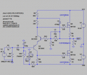
Somehow the God of Luck smile on you. A simpler solution was found. I tested a 1k8 resistor at the base of the NPN (R12 in attached schematic) helps to contain the cross conduction issue. Should be enough to protect against accidental > ~20V input. LtSpice asc included.... invite indra1 to contribute ...
You should test effectiveness and impact on sonic performance.
Attachments
Last edited:
- Home
- Amplifiers
- Solid State
- DLH Amplifier: The trilogy with PLH and JLH amps