I think these "long board" amplifier PCBs would be better if they were split into a long board output stage with a plug in PCB for the front end stage.
That leaves a compact optimally layed out front end and well spaced output devices again optimally layed out to minimise emi.
Dual inline plug and socket using anywhere from 2*6pins upto 2*10pins takes up little space. And leaves dual pin or quad pin parallel contacts for lower impedance, where the designer thinks that brings an advantage..
Last edited:
I am planing to build this amp with a powerfull psu.
I am puzzled by the 22ohm resistors parallel to the fuses.
If the fuses blow and the amp is driven at high power into a 8 ohm load, the 22 ohm resistors will need to dissipate more than 10watts so they will burn.
Why do we need the resistors ?
I am puzzled by the 22ohm resistors parallel to the fuses.
If the fuses blow and the amp is driven at high power into a 8 ohm load, the 22 ohm resistors will need to dissipate more than 10watts so they will burn.
Why do we need the resistors ?
Very interesting article: A DC Fault Protection Circuit for Audio Amplifiers
I am trying to figure out how and where the Honey Badger was improved since the build guide was written (I have the V2.4 boards).
Here are a few things I found in the main thread, but I am not sure if this is everything as the thread is a bit long:
- The addition of the Baker Clamp Diode ("D-BC" option): use a BAV21 or BAV20.
- R12 and R13 values (VAS CCS): use R12=6.8kΩ and R13=10kΩ (instead of R12=10kΩ and R13=15kΩ in the build guide).
- What's the "diode fix"? What needs to be changed where, how, and why?
Is this list complete? And what's the "diode fix"?
(And would it be a good idea to update the build guide?)
I just compared the resistor values in the V2.4 schematic shown on the diyAudio store with the parts list given in the build guide (also in the diyAudio store). I found the following differences (I may have missed some, and I haven't checked the caps and other parts):
- R3, R6 = 22 kΩ in the V2.4 schematic vs. R3, R6 = 33 kΩ in the build guide
- R23 = 47 Ω in the V2.4 schematic vs. R23 = 33 Ω in the build guide
- R24 = 1.5 kΩ in the V2.4 schematic vs. R24 = 820 Ω in the build guide
- R26 = 10 Ω in the V2.4 schematic vs. R26 = 100 Ω in the build guide
- R27 = 82 Ω in the V2.4 schematic vs. R27 = 68 Ω in the build guide
What's up with these? Should I use the new values from the V2.4 schematic or stick with the build guide? Why?
It would REALLY be nice to keep the build guide up to date and consistent with the schematic.
Here is my last schematic for the FET MOSFET HB that I am going to build.
It has all the latest mods captured in this thread and some differences.
The LTP CCS uses a led reference so it is stiffer than the two transistor model.
This CCS runs at 8.8mA so both input fets work at 4mA (2SK170 matched at 5mA Idss)
To avoid using a big transistor for the VAS I added the third transistor and to soften clipping I also put the BAV21.
The miller caps follow dadod input and the drivers do not use the caps as these might not be needed.
The fuse bypass resistors increased to 5k so they are sonicaly benefic but do not act as soft blow fuses.
The voltage spreader is now purely resistive and there are four 12zeners to protect the output mosfets.
D10 and D11 act as a poor man reg.
The LTP cascode reference is resistive and not connected to GND.
Any comments will be welcome as always.
best
Ricardo
Attachments
R26 should be 2k to 3k, or zero.
D1 &2 should be 1n400x
R49 << 10r
R30 may need a bit of experiment.
Be careful that you don't set the VR to exceed it's max current rating.
2000r @ 500mW gives an absolute max of 15.8mA
half power is 11.1mA
half current is 7.9mA
VR29. What direction do you want the adjuster to go to increase the output bias current?
Install the VR orientation so that you get that preferred direction.
The current injection from Q9 base should equal the current injection of the two Current Mirror bases. If not then the LTP ends up unbalanced. I think that is why your simulator is telling you to set R17 & R39 unequal. These two should be equal if the currents and voltages on the two LTP jFETS are the same.
Last edited:
There's a Thread running now that is discussing this potential oscillation.
The inductor needs a much lower resistance value to damp the ringing.
Unfortunately the sch does not allow direct measurement of these two injection currents.
But you can see an estimate by comparing the currents in the LTP sources using the Vdrop on the source resistors. But you can't do that because you have added the two unbalanced resistors.
You can measure the collector currents of the three BJTs and using the hFE you measured when selecting them, you can estimate the base currents and do a calculation to find the difference. (a lower hFE for the VAS helper EF helps to match these currents).
Alternatively you can add the third helper BJT between the two CM BJTs, then you use the extra resistor to trim the current match.
Last edited:
")
EXICON LateralsWhat output devices are you using?
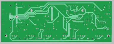
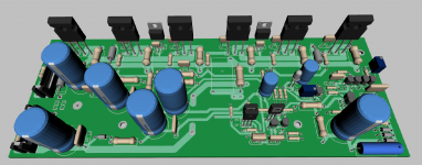
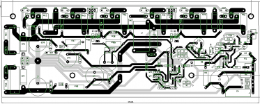
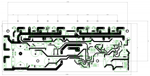
Finaly the layout..... as usual comments are welcome.
The power devices are far away from the PCB edge. How are you going to mount them to the heatsink?
- Home
- Amplifiers
- Solid State
- diyAB Amp - The "Honey Badger"