You can purchase an evaluation module for Analog Devices USB isolator for $50. This is a project where "make vs buy" comes into play.
Thanks Jack, The eval board is big and has many options that I do not need.This board is only 2x2 inch and can be made much cheaper that eval board. It is not 50$ about 65 plus shipping.
Sorry about the delay, we have had unaccustomed nice weather this weekend, so we decided to have a little break, so I have been happily absent from my computer all weekend.
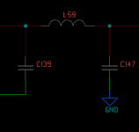
On the power +5 inputs of the USB I would suggest looking at a pi filter, with 2 caps and a ferrite, the 0V just having a ferrite.
This allows the input and output to be totally isolated by the layout. the layout below shows the isolated grounds split down the centre of the ferrite, this would apply if only ferrites are used and the same split should go under the common mode choke.
Sorry I haven't done more, but couldn't resist the weather")
On the power +5 inputs of the USB I would suggest looking at a pi filter, with 2 caps and a ferrite, the 0V just having a ferrite.
This allows the input and output to be totally isolated by the layout. the layout below shows the isolated grounds split down the centre of the ferrite, this would apply if only ferrites are used and the same split should go under the common mode choke.
Sorry I haven't done more, but couldn't resist the weather
Attachments
Marce ,Please find the attached board. I am not sure if you saw the eagle board file.
Did you mean the 5V at peripheral side? The bus side is totally isolated and I guess power supply filtering is not needed.
On the peripheral side on the other hand will need a dedicated power supply if the isolator is for audio and should also provide power for DAC.
So is it not a good idea to keep the filtering part on PS board and ferrite just working as differential mode chokes in power line to filter out any residual RF noise picked up by power supply cable?
Attachments
I'll draw it out better tonight as it will be easier than trying to explain.
By the way USB lines should be routed as 90ohm diff pairs with close length matching preferably, getting 90ohm diff on a double sided board is almost impossible, but routing as a close coupled diff pair should be used.
By the way USB lines should be routed as 90ohm diff pairs with close length matching preferably, getting 90ohm diff on a double sided board is almost impossible, but routing as a close coupled diff pair should be used.
FR4 high temperature substrate, with a dialectric constant of 4.6 at 1MHz.
It's .063 inches (1.6mm) thick, with 1oz (35um) copper on both sides.
The manufacturers spec of PCB and on calculation. The traces should be at least 40 mills with 16 mills gap between conductors to get differential impedance close to 90. I used Saturn PCB calculator.Now I understand why it is not that easy.
Last edited:
Diagram to illustrate the ground split shown above. Will try and throw together a layout later.
You can also use this for impedance calculation:
http://www.skottanselektronik.com/
You really want 90 Ohm diff pair, impossible on a two layer boards, it wont make that much difference in the real world with USB2.
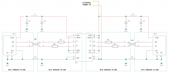
The Pi filter caps want to be above their respective ground planes on the PCB.
I have left off the transient suppression diodes (e.g. SRV05-4A) these can be added for extra protection.
You can also use this for impedance calculation:
http://www.skottanselektronik.com/
You really want 90 Ohm diff pair, impossible on a two layer boards, it wont make that much difference in the real world with USB2.
The Pi filter caps want to be above their respective ground planes on the PCB.
I have left off the transient suppression diodes (e.g. SRV05-4A) these can be added for extra protection.
Attachments
Last edited:
But why directly before/after an isolator chip, surly any common mode noise is'nt going to be generated on the isolators output side?
The noise radiates in both directions. Each and every cable is a transmitting antenna.
http://www.analog.com/static/imported-files/circuit_notes/CN0158.pdf
Last edited:
Yep, its an EMC thing, as the design I have put up for the OP to peruse is based on what we do on military/medical/aerospace boards and passes some stringent EMC tests, I think it would be suitable for a DIY Audio designs. As I said in an earlier post I have also omitted the SRV05-4A or similar transient suppression diode package.
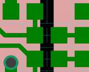
if you look at the ground planes and there positions on the schematic you will see that when laid out correctly the noise has quite a few barriers to get through. And laying out correctly is the key to getting the maximum noise immunity and isolation. I showed a bit of a layout earlier, that shows the 0VA/0VB split down the centre of the supply ferrites and also the common mode choke. This is designing for as near as possible ultimate EMC protection (and thus noise reduction).
if you look at the ground planes and there positions on the schematic you will see that when laid out correctly the noise has quite a few barriers to get through. And laying out correctly is the key to getting the maximum noise immunity and isolation. I showed a bit of a layout earlier, that shows the 0VA/0VB split down the centre of the supply ferrites and also the common mode choke. This is designing for as near as possible ultimate EMC protection (and thus noise reduction).
Thanks Marce, I figured there are some bypass caps missing. But all these new caps after inductors how do you decide on their value.
And for USB data signals which is more important the symmetry between D+ D- layout or the length. For now I meander the tracks and they are close to 30mils in length difference.
And for USB data signals which is more important the symmetry between D+ D- layout or the length. For now I meander the tracks and they are close to 30mils in length difference.
Both are important...But coupling (ie diff pair routing) more than length matching, length should be around 100ps, so 3.8mm (0.150" for those living in the Dark Ages )
What track and gap have you gone for?
Ah! the pi filters, they give much better attenuation than just ferrites on their own. 680p with some 1300r/550Mhz ferrites are a popular mix.
)What track and gap have you gone for?
Ah! the pi filters, they give much better attenuation than just ferrites on their own. 680p with some 1300r/550Mhz ferrites are a popular mix.
Last edited:
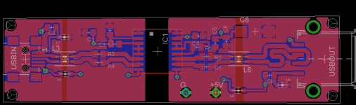
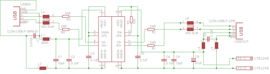
here is the updated board. I am not sure if I have to isolate the v bus plane in addition to the ground plane?
Marce can you please help me with ferrite and capacitor selection. I used the wurth we-CBF 0805 in this board( as the eagle library was available).
Hope you can pick one from that series.
Marce can you please help me with ferrite and capacitor selection. I used the wurth we-CBF 0805 in this board( as the eagle library was available).
Hope you can pick one from that series.
Attachments
Yes that is critical to noise suppression. Any noise from a computer or other source that the USB comes from is going to be mainly high frequency. The main coupling method for this high frequency noise is capacitive (this is one of the areas that many forget when laying out PCBs, capacitive coupling of high frequency noise) so having a clean plane under a noisy plane negates the split.
I would have the bottom layer for ground and ground planes only and would route the power on the top layer as tracks. Again this gives the best shielding and return paths for all the signals and further minimises noise problems as the capacitive coupling between the power and the ground is minimised. Again, think of your 5V USB supply from a PC, this is the most likely candidate to have noise present. You cannot guarantee that the host device has good clean power especially if it is a PC as these are often built down to a cost, so treating this line as a possible source of noise is paramount. That is the main thing I wanted to show in the schematic above, the 5Vs being filtered by a PI filter, and a distinct break between input and output over 3 barriers.
I would have the bottom layer for ground and ground planes only and would route the power on the top layer as tracks. Again this gives the best shielding and return paths for all the signals and further minimises noise problems as the capacitive coupling between the power and the ground is minimised. Again, think of your 5V USB supply from a PC, this is the most likely candidate to have noise present. You cannot guarantee that the host device has good clean power especially if it is a PC as these are often built down to a cost, so treating this line as a possible source of noise is paramount. That is the main thing I wanted to show in the schematic above, the 5Vs being filtered by a PI filter, and a distinct break between input and output over 3 barriers.
- Status
- This old topic is closed. If you want to reopen this topic, contact a moderator using the "Report Post" button.
- Home
- Source & Line
- Digital Line Level
- DIY USB isolator