Phases
Hi All,
I don't think we need to split the thread or projects. Lets just do this in phases that allow some of our members to get off the train at an earlier stop.
Here is a proposed phase description:
Phase 0: Basic Operation
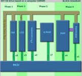
Block Diagram
Power Supply (separate control, cd-rom driver, cd-rom control)
Test the basic operation using cd buttons (if it has them) and digital/audio out.
A performance evaluation should be done so that we have a baseline for the more advanced phases.
Phase 1:
MCU and new buttons replaces stock buttons
Phase 2:
LCD
Phase 3:
IDE digital out
Added LCD functionality (Index etc)
Compare performance
Phase 4:
Buffered IDE digital out
DAE
compare performance
Phase 5:
Enhanced Clock with external output
compare performace
Phase 6:
MP3 and other formats
I do not see that phase 3 is completely redundant as it accomplishes the digital transmit, clock, and serial to parallel conversion all of which has to be done for Phase 4 and with DAE we only have to change the commands sent to the drive.
Please suggest changes to these phase descriptions!!!
Gregory
Hi All,
I don't think we need to split the thread or projects. Lets just do this in phases that allow some of our members to get off the train at an earlier stop.
Here is a proposed phase description:
Phase 0: Basic Operation
Block Diagram
Power Supply (separate control, cd-rom driver, cd-rom control)
Test the basic operation using cd buttons (if it has them) and digital/audio out.
A performance evaluation should be done so that we have a baseline for the more advanced phases.
Phase 1:
MCU and new buttons replaces stock buttons
Phase 2:
LCD
Phase 3:
IDE digital out
Added LCD functionality (Index etc)
Compare performance
Phase 4:
Buffered IDE digital out
DAE
compare performance
Phase 5:
Enhanced Clock with external output
compare performace
Phase 6:
MP3 and other formats
I do not see that phase 3 is completely redundant as it accomplishes the digital transmit, clock, and serial to parallel conversion all of which has to be done for Phase 4 and with DAE we only have to change the commands sent to the drive.
Please suggest changes to these phase descriptions!!!
Gregory
Konnichiwa,
It makes no difference. The use of DAE and all the rest exist primarily to avoid using the Drives S/P-DIF output which is invariably dreadful on all but a few very old Drives.
And by using asyncronous DAE we can als re-read sections which would normally cause the error correction to "correct" (read interpolate) sectors with bad checksum. On 2nd or 3rd read such sections often read fine.
This is IMNSO also one of the reasons for the sometimes noted improvement of PC Sourced CD Copies. Most decent rippers will re-read until a pre-specified number of attempts before interpolating. I have some badly scratched CD's which on most CD-Players simply drop out occasionally (my DVD Players also tends to play with zero dropouts BTW!). Yet the copies from the same CD done using EAC allowed Zero Errors (meaning EAC never used interpolation but eventually got valid data) and play without a hitch and predictably much better sound.
So the whole point is to get the raw data and send it to following devices under explicit control with full control over the timing (Jitter etc).
BTW, some older DVD Players operate CD Repaly like that and make excellent Transports once fitted with a suitable clock.... Oh, and Meridians best work that way too.
Sayonara
HBarske said:Not sure if this helps us here, but:
CD data is already buffered by the drive itself. Modern drives all seem to have 128 kilobytes of buffer memory.
It makes no difference. The use of DAE and all the rest exist primarily to avoid using the Drives S/P-DIF output which is invariably dreadful on all but a few very old Drives.
And by using asyncronous DAE we can als re-read sections which would normally cause the error correction to "correct" (read interpolate) sectors with bad checksum. On 2nd or 3rd read such sections often read fine.
This is IMNSO also one of the reasons for the sometimes noted improvement of PC Sourced CD Copies. Most decent rippers will re-read until a pre-specified number of attempts before interpolating. I have some badly scratched CD's which on most CD-Players simply drop out occasionally (my DVD Players also tends to play with zero dropouts BTW!). Yet the copies from the same CD done using EAC allowed Zero Errors (meaning EAC never used interpolation but eventually got valid data) and play without a hitch and predictably much better sound.
So the whole point is to get the raw data and send it to following devices under explicit control with full control over the timing (Jitter etc).
BTW, some older DVD Players operate CD Repaly like that and make excellent Transports once fitted with a suitable clock.... Oh, and Meridians best work that way too.
Sayonara
I still like the idea of the DIY DAE unit. Though how universal is the DAE standard !? I know that many audio grab programs have a huge amount of settings for optimal grabbing!!!
BTW: what about the idea of using a PC with an external DIY USB soundcard with good clock/reclocking !? This way also MP3's and software samplers (gigasampler) can be used. And the user interface is much better of course...
Fedde
BTW: what about the idea of using a PC with an external DIY USB soundcard with good clock/reclocking !? This way also MP3's and software samplers (gigasampler) can be used. And the user interface is much better of course...
Fedde

I2S conversion
I just wanted to run thru this timing and see if I understand it correctly.
First, I2S is simply 16bits of L followed by 16bits of R with a serial clock and a LR clock that switches states depending on whether the data is L or R.
Assuming we have done everthing else and we have a position in ram begining our data and a function to extract just the L and R data.
The timing of 32 bits is 1/Fs and assuming Fs = 44100 is:
that means we have to transmit 32 bits in 22.68 us
So our serial clock period would be 22.68 us / 32 or 708.6ns
or 1.4112 Mhz and the left/right clock would be 88.2khz or
11.3 us
if our MCU is 33mhz and its instruction time is 1/1 each instruction would be 30ns.
So... do we have only 23 instructions in which to do everything?
What am I doing wrong?
If we simply clock this out without intervention we would still have to do the ram addressing and control the rd/w control pins in this time frame would we not?
Gregory
Re: I2S conversion
Konnichiwa,
I actually figured on halve that. I suspect the solution lies in multiple uP's and a shared global memory (classic PC/Mac Architecture) where the drive controller fills the Memory with Data and conrols the IDE Bus, a second controller (much more primitive but fast) that applies the memory reads and another controller for the Buttons, Display and overall control.
Probably a 33/50MHz 16 Bit processor to control the Drive and another to read out the data on external clock and manage buffer size, plus an 8Bit/8MHz dinosaur to coordinate the shooting match...
Sayonara
Konnichiwa,
gregorx said:So... do we have only 23 instructions in which to do everything?
I actually figured on halve that. I suspect the solution lies in multiple uP's and a shared global memory (classic PC/Mac Architecture) where the drive controller fills the Memory with Data and conrols the IDE Bus, a second controller (much more primitive but fast) that applies the memory reads and another controller for the Buttons, Display and overall control.
Probably a 33/50MHz 16 Bit processor to control the Drive and another to read out the data on external clock and manage buffer size, plus an 8Bit/8MHz dinosaur to coordinate the shooting match...
Sayonara
Thorsten and All,
This is kind-of what I have been saying for a few days. This can not happen with a high level language and now, even with a single processor.
Perhaps we could do the conversion in gates or with an FPGA but still 23 instructions in a single 8bit uC just isn't going to happen.
Using multiple processors would work but that shared memory is going to be a real pain in this short number of instructions. Even highly optimized assembler code would require quite a few instructions to assemble addresses and moving 16 bits arround is no walk in the park.
Is there some sort of IDE or Memory controller chip that we might utilize to solve this issue?
Perhaps there is a way to use the peripherals in some uCs to control the pulses. We could easily use a PIC in SPI mode to generate the serial clock, transmit data, and an extra pin or maybe PWM mode to create the LR clock. Here the Harvard Architeture rules... Then the only instructions required are addressing and moving memory and controlling the bus. Still a tall order....
I want this DAE/Buffer thing to work, I just find that trying to identify and solve the complicated issues upfront make for more successful projects.
Still using a phased design with the easy stuff working and breadboarded we might encounter a solution and be able to expand into the advanced phases.
There has to be a better solution than building our own PC.
Lets put our heads together and figure it out.
Gregory
The "better" solution certainly is the use of a DSP. As many of them already feature I2S outputs. the generation of the digital audio stream should not be too difficult.
BUT: We are talking of 200 pin SMDs (fine pitch), four layer boards, critical board leyout,...
Is it that what we want...?
BUT: We are talking of 200 pin SMDs (fine pitch), four layer boards, critical board leyout,...
Is it that what we want...?
All:
My Samtec IDE connectors came this morning, and they are *very* nice. Nice enough that I would consider replacing the IDE connectors on the CDROM with them.
Part numbers:
TST-120-04-G-D-RA ("normal" solder leads as far as I can tell)
TST-120-05-G-D-RA (slightly longer solder leads than above)
My Samtec IDE connectors came this morning, and they are *very* nice. Nice enough that I would consider replacing the IDE connectors on the CDROM with them.
Part numbers:
TST-120-04-G-D-RA ("normal" solder leads as far as I can tell)
TST-120-05-G-D-RA (slightly longer solder leads than above)
Konnichiwa,
I may be wrong here, but the original CD-Players included tons of hardwired CMOS Logic, which in those days was pushing things with 20MHz clock speeds. So, if 20 years ago we could handle thing near discrete, where is the ******** problem nowadays?
I believe IDE interface chip's exist off the shelf, they should be able to handle putting the data into our buffer, simply by being told "fill memory location XXXX to YYYY with a block of audio data from the CD now".
There are no doubt other special use IC's. Maybe the study of these various MP3 HDD Player projects might give some clues?
Sayonara
HBarske said:The "better" solution certainly is the use of a DSP. As many of them already feature I2S outputs. the generation of the digital audio stream should not be too difficult.
BUT: We are talking of 200 pin SMDs (fine pitch), four layer boards, critical board leyout,...
I may be wrong here, but the original CD-Players included tons of hardwired CMOS Logic, which in those days was pushing things with 20MHz clock speeds. So, if 20 years ago we could handle thing near discrete, where is the ******** problem nowadays?
I believe IDE interface chip's exist off the shelf, they should be able to handle putting the data into our buffer, simply by being told "fill memory location XXXX to YYYY with a block of audio data from the CD now".
There are no doubt other special use IC's. Maybe the study of these various MP3 HDD Player projects might give some clues?
Sayonara
No. The ATA interface is nothing but a 16 bit wide data bus plus some control registers. Interfacing this to any kind of processor/controller is no big deal.I believe IDE interface chip's exist off the shelf
Things are starting to become interesting if you increase the speed of the data transfer. Modern CD ROMs already use the UDMA-33 interface. This was state-of-the-art on interfacing a hard disk drive just a few years ago.
20 years ago there was no DAE.So, if 20 years ago we could handle thing near discrete
Is 32 kbytes of RAM enough?Maybe the study of these various MP3 HDD Player projects might give some clues?
@Name:
The CDROM will produce a very jittery and electrically noisy signal full of mis-reads if we trace to just before the onboard DAC. Our DIY version will have power supplies that produce near or less electrical noise than batteries, will be jitter free, and have no mis-reads under good conditions.
The CDROM will produce a very jittery and electrically noisy signal full of mis-reads if we trace to just before the onboard DAC. Our DIY version will have power supplies that produce near or less electrical noise than batteries, will be jitter free, and have no mis-reads under good conditions.
Re: Phases
thanks for the pioneer product no.
yes, this is exactly what i wanted could i miss out steps 4 and 5?
also, could someone point out a good DIP package DAC IC? one that i can get samples of. thanks.
[EDIT]: from Texas Instroments. i have just looked at their sitem and they have hundreds. how many bits should i be looking at? 8? 16? 20?
thanks for the pioneer product no.
gregorx said:Hi All,
I don't think we need to split the thread or projects. Lets just do this in phases that allow some of our members to get off the train at an earlier stop.
Here is a proposed phase description:
Phase 0: Basic Operation
Block Diagram
Power Supply (separate control, cd-rom driver, cd-rom control)
Test the basic operation using cd buttons (if it has them) and digital/audio out.
A performance evaluation should be done so that we have a baseline for the more advanced phases.
Phase 1:
MCU and new buttons replaces stock buttons
Phase 2:
LCD
Phase 3:
IDE digital out
Added LCD functionality (Index etc)
Compare performance
Phase 4:
Buffered IDE digital out
DAE
compare performance
Phase 5:
Enhanced Clock with external output
compare performace
Phase 6:
MP3 and other formats
I do not see that phase 3 is completely redundant as it accomplishes the digital transmit, clock, and serial to parallel conversion all of which has to be done for Phase 4 and with DAE we only have to change the commands sent to the drive.
Please suggest changes to these phase descriptions!!!
Gregory
yes, this is exactly what i wanted
could i miss out steps 4 and 5?also, could someone point out a good DIP package DAC IC? one that i can get samples of. thanks.
[EDIT]: from Texas Instroments.
i have just looked at their sitem and they have hundreds. how many bits should i be looking at? 8? 16? 20?I'm afraid those are all non-audio DACs.
If you would like to go with TI (formerly Burr Brown), you might have a look here: http://focus.ti.com/docs/search/par...am_table&templateId=5275&showAssociated=false
If you would like to go with TI (formerly Burr Brown), you might have a look here: http://focus.ti.com/docs/search/par...am_table&templateId=5275&showAssociated=false
@Matttcattt:
I just received a bunch of TI/BB DACs this morning. I hope you can handle soldering SSOP packages... they are so tiny... The only ones I got that are not in SSOP packages are PCM1710, but they are still surface mount. Just not *as* hard to solder. You could use Philips TDA1543, which is only 8 pin DIP, and costs like $2.00, and is very easy to implement. I think I might do this as well...
I just received a bunch of TI/BB DACs this morning. I hope you can handle soldering SSOP packages... they are so tiny... The only ones I got that are not in SSOP packages are PCM1710, but they are still surface mount. Just not *as* hard to solder. You could use Philips TDA1543, which is only 8 pin DIP, and costs like $2.00, and is very easy to implement. I think I might do this as well...
separate CPU
Read the previous posts just now, It's way to hot here to do anyting substancial now.
Regarding using more than one CPU. I was thinking about using a small pic processor for decoding the infrared part. When the system is idle only this part should be connected to the power. Whenever yuo switch the system on by remote the pic switches the rest of the system on.
Regarding the output buffer. You need something that has asynchronous in and synchronous out. Might be that there are standard chips already for this. Par to ser converters or something like that.
MGB
Async in, sync out can be done with an asynchr. fifo. This is a first in - first out buffer with 2 independant clocklines to clock data in and clock data out.
The problem is that the clocks need to be at the same freq, otherwise the fifo will run full or empty. I said same freq, not same jitterspec!!!! So you can remove jitter by clocking out on a good xtal and feed the clock back to the transport (like my dac).
Next problem is that dac clock needs to be equal to transport clock (or e.g. in my case dac = transport/div4).
But there is one other way: If the input clock has no relation with the output clock, you need indications on buffer full/empty and speed up/slow down the transport clock. One might put two fifo's after each other as one big fifo and then use the half full flags of both to determine to speed up/down the incoming clock.
first fifo half full = speed up
last fifo half full = slow down
Or to keep closer to your project:
first fifo half full = start dataflow
last fifo half full = stop dataflow
Greetings,
GuidoB
- Home
- Source & Line
- Digital Source
- DIY CD drive based on a computer CDROM