me said:how does flipping the phase (180 degrees) of a 2kHz signal make any difference relative to the 1kHz signal that it was born from?
That was poorly phrased. Consider that the 1kHz signals presented to the grids of the PP pair are 180 degrees out of phase relative to each other. Now we add the 2kHz CM signal to both grids. The phase (+/-) of the 2kHz signal should make no difference ....
Hi Don,
Thanks for working your brain on this one
If I check but think voltage and use an arrow to show the result, I get the following:
see att. and start at V cause, which goes up
Now it works in my view
Thanks for working your brain on this one
smoking-amp said:Hi Mark,
Quick check: If an output is supplying too much gain, the current thru rk2 will increase, this works its way back thru Cf and the input xfmr to the driver grids to raise CM conduction there. Increased tail current then increases driver gain. But we need a complementary decrease in driver gain to compensate the increase of the output tube. Back to drawing board.
Don
If I check but think voltage and use an arrow to show the result, I get the following:
see att. and start at V cause, which goes up
Now it works in my view
Attachments
Hi Dave C.
First, what I meant by common mode signal inverted is that an increase in total conduction of the tubes will pull the common mode voltage of the plates down (assuming some resistance in the xfmr) and will pull the common mode voltage of the cathodes up (assuming some tail resistance). So the common mode voltages are inverted between the two.
I believe your description using balanced mixer theory/frequency domain can be made consistant with the time domain picture I have used. See below for an attempt.
As to the difference in phase of the 2nd order products mattering, imagine the 2nd order distortion being made by one output tube OR the other output tube acting a little stronger in its SE mode. The correction required will be different depending on which polarity of the input signal is causing increased conduction. So phase does matter. Well its clear in the time domain anyway. I think in the frequency domain you will see a sign inversion of the 2nd order products depending on which tube causes it. Similarly for 3rd order products, the conduction could be increasing toward max +/- signal or it could be increasing around zero crossing. So phase will matter here too, different corrections required.
Next, let me clarify the picture some in the time domain. For ideal linear devices the common mode current (class A of course) will stay constant versus signal. Similarly it stays constant for square law devices like Mosfets since an increase of transconductance or conduction of one device is equally offset by a decrease in the other device. Since the two devices are effectively in parallel for class A operation, the sum is all that matters.
Now any deviation from this constant total transconductance will show up as a variation of the common mode current. So we can measure total output stage transconductance variation this way and use it to oppositely vary total transconductance (or gain effectively) in the previous stage to preserve a constant gain product. So the driver stage is acting as a complementary gain modulator to whatever the output stage is inadvertantly doing with its gain.
(In class A P-P with identical output devices we would expect to only see odd order variations occur in the CM signal, but the scheme is actually able to correct even order ones too. So the description as an Odd Harmonic canceller is a little oversimplified.)
Both output and driver stages are thus balanced modulators. So whatever frequency domain products the output stage is generating, the input stage is doing the inverse operation. Since they are out of order regarding the signal flow, the remaining question would be whether the maths support transposing the ordering of the two functions as equivalent. I believe this is allowed (as long as there are no phase deviations occuring in the two functions, no energy storage). Often called pre-distortion followed by distortion to get constant gain. The bandwidths of the correcting device and output stage must clearly be well above the audio range to avoid phase effects in band.
Mark:
Looking at Marks signal flow diagram, I now see where the confusion is arising. And true indeed, this configuration will restore the initial common mode voltage variation to zero just like a negative feedback loop. However, this is not the goal. The output stage is allowed to distort in its own merry way, we are not fixing it. The initail CM error signal should remain. We are using the Cm variation signal to operate the complementary gain variation of the driver stage. So the variation seen on the CM signal path with a scope will be a non zero one and will be an indication of how much pre-distortion the driver is performing at any given moment. Now reversing the common mode signal polarity from Marks diagram, will actually increase the origianl CM variation some, but it is a small effect. The loop gain here is only enough to correct a few % typical error.
Now, for a single stage error correction scheme, assuming it works, this would be different. We would expect the common mode signal to remain constant (or nearly).
I don't recall the Bell Labs/Kreer patent mentioning anything about connecting output CM signals to input CM signals. This seems to be something different in the WE92A.
Don
Problems, fixes, CCS?
Marks example has just woken me up to a problem that needs fixing. Changing the tail current thru the driver stage (by either cross coupled feedbacks to the driver grids or by modulating a tail CCS) causes a common mode voltage shift to propagate from the driver plates to the output grids. This makes the output tubes bias shift in the wrong direction (for error correction to the gain) dynamically. So we need to stop the common mode shifts on the driver plates by loading them with a center tapped inductor to their B+. Not real attractive, but do-able.
Thinking a bit more (very dangerous), what if we try doing the correction in the output stage itself. We would monitor the common mode current (cathode or plate), and instead of modulating the differential grid drive signal amplitudes, as the driver stage scheme did, we would vary the tail current in the stage by adjusting the common mode grid bias (just like we did to the drivers before to vary their gain).
I think what ends up happening here is we will correct back to a constant CM current. So we could just put a CCS in for a cathode tail. Unless it turns out that we need to correct more than back to the norm, then we could try a negative resistance tail, possibly unstable.
Using a CCS tail clearly does improve distortion significantly, but at high amplitudes, like in an output stage, it inevitably makes some odd order distortion still. So would a negative resistance in the tail fix this?
Don
It looks to me that the cross coupled driver stage scheme (or modulated CCS driver) can correct to complete unity error correction without instability since we can just adjust the gain pot thru null, but a single stage "corrector" or CCS cannot quite fully correct the errors it seems. But comes close. Now I am trying to think of something that would bridge the slight shortfall.
With a CCS, the current stays constant, so we cannot use a CM resistor in the xfmr B+ lead (like the Kreer patent) to any effect. But the common cathode connection or tail voltage on the CCS does vary in voltage some with signal. And I know there are some SS schemes that make use of this voltage for correction.
Let's look at the operation of a differential tube pair with CCS tail.
The combined transconductance curve for the two tubes is not quite constant, but droops off with larger signal (away from zero difference) until it finally drops off drastically with saturation setting in. The tube which is turning off generally turns off slower and slower as differential amplitude increases due to dropping MU. So as a consequence the CCS increases the tail voltage to speed it up so the other tube can get its increased current. So the tail voltage is increasing as the gain droops.
Now we can increase the gain by increasing the CCS current, and an increased CCS current would pull the cathode voltages down some (to turn on the tubes more to draw the extra current). Seems like a natural fit, they track.
So first attempt would be monitoring the CCS/cathode voltage and modulating the CCS current to keep the CCS/cathode voltage constant. But we know that a constant cathode voltage is noticeably distorting, and is equivalent to a zero Ohm tail resistor, so this is too much fixup.
Next attempt would be something in between, a finite (likely high) resistance in parallel with the CCS would allow the current to increase some as tail voltage increases, but this would not hold the voltage constant. Tail voltage would increase somewhat less than the uncorrected case though. If this linearizes gain successfully, then it would indicate that a CCS was to much gain fixup in the 1st place.
Next case that I can think of would be a non-linear resistance in parallel with the CCS, like a thermionic diode or a triode with an unbypassed cathode resistor, like the top triode used as a load for the Aikido input stage (essentially an adjustable diode). Actually, this is just equivalent to a poorly performing triode CCS.
I think I would just try a high value resistor in parallel with the CCS as my first test. Then try a high Rp triode CCS.
Well, have I driven everybody nuts yet? Time for beddie-bye time here. Sleep on it.
Don
smoking-amp said:
Well, have I driven everybody nuts yet? Time for beddie-bye time here. Sleep on it.
Don
Well, yes.
It is getting a bit over my head now
I'll study this first for a while before getting back to you...
"Don, I'm waiting now till you come to a resistor in parallel with no CCS... "
Well, my latest calculations indicate a tail impedance of 9.784562% less than infinity. (but 9.784563 % won't do it) This will obviously require a very complex and expensive circuit to achieve.
But you may be right. Just a resistor might do it.
"Well, yes."
I have probably confused the issue by investigating the single stage corrector case too. The two stage corrector (driver pre-distortion) wants to leave the CM current signal undisturbed, and runs with a finite (trimpot adjusted) gain from it. The single stage corrector does indeed try to correct the CM signal back to zero variation, apparently collapsing to just a CCS tail circuit or close to it.
Don
edit: It would be nice if we could get both schemes to work at once, ie. pre-distort and single stage correction. Unfortunately, the common mode loop thru both stages does opposite corrections in each when using N channel devices for both (tubes). But if we were to replace the driver stage with P- Mosfets, I think we can get both effects properly aligned (and get rid of the center tapped driver stage load inductor). Stay tuned.
Assuming the schematic in post #31 by jkeny is a clone of the "Baby Huey", it would seem a simple mod to convert the CCS to work like the scheme in post #37 above.
This is Gingertube's original schematic for the ECL86 variant (the first baby Huey). There were other schema that followed based on different tubes.
I would indeed be interested if it was possible to mod the above Baby Huey schematic into a cross-coupled compensator while retaining the partial feedback of the Baby Huey circuit. Looking forward to how this all pans out!
"how this all pans out!"
Not panning out too well lately, unfortunately.
After looking at the failure of a CCS loaded LTP to fully correct odd harmonics, I have realized the the two stage corrector suffers from the same problem. This is becuase the tail current is NOT a LINEAR function of transconductance variation. For a tube (using the 3/2 power formula):
gm = K(Vg+Vp/Mu)^0.5 = K'(Ip)^0.3333
So odd harmonics are encoded in the tail current, but not linearly. This means that our driver stage is NOT generating an EXACT inverse gain function (at least not for large variations). This is also the reason gm does not stay constant with a CCS in the tail of an LTP. So we are not likely to do any better with the two stage corrector than a CCS loaded LTP.
The difficulty of making a linear corrector is now at LEAST an order of magnitude more difficult. Probably requiring a textbook sized treatise to solve it.
The square law MOSFET LTP however does behave sufficiently well since its transconductance is gm = K(Vg) and sums linearly to a constant between the two halves of the LTP when differentially driven.
OH, I did determine that a P-channel Mosfet driver stage can be arranged to do both 2 stage and single stage error correction simultaneously. (ie. one can get the all three feedbacks aligned: conventional diffl. NFDBK, common mode loop, and common mode to diffl. gain loop)
There is actually a "FORTH" feedback mechanism, not considered so far. This would be diffl. feedback to common mode gain effect. Maybe it is the key to solving this mess, since it is the effect showing up in the tail voltage variation of the CCS/LTP with diffl. signals. And that variation looks like a key to at least patching that up.
At this point I think I would just fallback to trying to patch up the problem in the CCS loaded LTP rather than trying to fix the two stage corrector. Although, there is likely some elegant solution to it lurking out there somewhere. But since the one stage corrector (or CCS loaded LTP) is related to it, any solution to it, I would try working backwards towards or split apart or something such to find the two stage solution later.
Don
some tools for the adventurous:
to experiment with various "patches" I will just throw out some ideas I have come up with:
1) the center tapped inductor load for the driver stage can block common mode signals from getting back to the output grids. (ie. replace R5 and R5' in the earlier two stage schematic.) Or, P-channel drivers can invert the common mode signal loop to agreeably align it with the error corrector stage effects without the inductor required.
2) high resistance across a CCS or non-linear CCS (triode or Mosfet with a reference feedback)
3) the two stage (driver stage) inherently uses attenuators from the plate outputs back to the driver grids, how about using two triodes in reverse as attenuators. ie, output tube plates drive the plates of small triodes that are grounded grid, with CCS loads on their cathodes. Gives 1/Mu attenuation signals on the cathodes with some small non-linearities.
4) try using the "FORTH" feedback (the dark force!), by putting a CCS on the driver tail, and monitor the CM voltage on the outputs to control a current source to modify driver tail current. This would attempt a tracking or inverted voltage on the driver tail (using either an Rsense in outputs tail or a CCS in outputs tail for the control voltage pickoff)
5) Screen feedbacks on the drivers are more linear than the grids, so would have some non-tracking linearity difference with the forward diffl. signals on the driver grids. This provides a useful 1/Mu_screen effect for attenuation and is more DC compatible with the output plates too. This probably gives similar results to using the inverted triode feedbacks (#3).
6) Just use Mosfets for the outputs with a CCS. (OK, that's cheating!)
Don
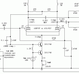
Hi Don,
I have no bright ideas atm, but found some more cmfb schemes, maybe they can give some inspiration?
One is here, by Fred Nachbauer
http://www.dogstar.dantimax.dk/tubestuf/driver02.htm
Attached another one that is on my hard drive, of which I don't know the origins, but has the same functionality.
These can maybe work for an outputstage just as well.....
Attachments
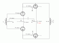
Mark,
Your common mode feedback stabilizer post just gave me an idea that can get rid of the center tapped inductor plate load for the drivers (for stopping the common mode signal from getting to the output tube grids when using an N-type or tube driver stage).
The R5,R5' (or RL,RL') resistors in the earlier schematics get tied together, and a common mode resistor connects from their junction to B+. The junction then gets controlled by a modulated Mosfet stabilization servo to keep the common mode voltage on the driver plates constant. I'll work up a schematic tomorrow.
Also, I now believe I see at least three or four workable ways to close the gap on the remaining bit of odd order distortion. (which CCS/tail correction leaves and the two stage corrector also seems to suffer from since it uses the same output tail current for control)
We need just a tiny bit of additional characteristic curvature non-linearity to modify the corrector action. And it needs to be adjustable for fine tuning it. Several ways present themselves.
(The single stage corrector or CCS/tail cannot utilize this since the error causing stage and error correcting stage are one and the same, so have the same curvature.)
1) By adjusting the idle current in the driver/corrector stage we can influence the Mu non-linearity of the driver if the tube has an increasing Mu curve versus idle cathode current. Many tubes meet this criteria with a peak occuring in the Mu at some current.
The common mode feedback has to be thru a modulated CCS for the driver so that it is not equally effected by the changing Mu (or the varying Mu would do nothing except slightly alter open loop gain). Simple pot adjustment of CCS idle.
2) The screen grid (pentode driver/corrector) is much more linear than the g1. By adjusting the cross-coupled feedback ratio between screen grids and grid 1s of the driver, we can change the Mu curvature. Note that by putting the feedback on the more linear screen grid and the forward signal on the g1s, that an increasing variation in g1 Mu causes less feedback effectively and so more forward gain. Similarly, we can adjust the idle current for a suitable curved Mu tube to adjust non-linearity here. Giving a 2 dimensional adjustment of non-linearity.
3) A Mosfet has a characteristic curve that varies from square law at moderately low currents thru 3/2 power at moderate current to nearly linear at high current. The P-channel differential Mosfet driver scheme can make use of this by again varying idle current of the P-Mosfet driver.
4) Since the P-channel scheme operates with both 2 stage and 1 stage error correction, (and one stage is identical to CCS/tail effectively), we can vary the Mu curve by adjusting how much correction is done in the corrector stage versus how much is done by common mode feedback to the output tubes (assuming the corrector stage has a different linearity curve than the output tube). Variation is done by adjusting a common mode stabilization servo for the driver "plates". Also CCS idle current can be adjusted for the corrector stage. Giving 2 dimensional adjustment of non-linearity.
Our cup overflows. I will try to put some schematics together tomorrow if time allows.
Don
5) Using a pentode for the driver/corrector we could vary its operation between triode and pentode mode by adjusting how much the screens follows the plates (Mosfet screen drivers, zeners, pot....)
The pentode and triode have opposite sign 3rd harmonic terms, maybe the higher odd terms too. This would change the driver/corrector curvature characteristic in an interesting way.
We could even bridge the adjustment pot between the output tube plates and the driver tube plates. Ultralinear to anti-ultralinear screen signal. OK, I have NO idea what that one will do.
Whoa! (--sound of a tube blowing up in the background!--)
Don
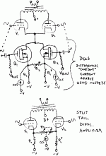
Differential CCS!!!!
The previous 5 fixups were in the realm of patch-ups as I had earlier suggested. And I think it is likely some can be made to work well. But they depend essentially on mis-matching transconductance curves between different devices or operation modes and on adjusting how much mis-match we want while observing with a spectrum analyzer. The next scheme(s) are more in the nature of a theoretically justified fix-up, which do not need slightly different gain devices or modes.
The reason a CCS does not work fully to correct odd order distortion of an LTP is due to the tail current being composed of two components summed which are each 1/3 power related to the complementary inputs (for tubes). This means that a small range of gains are possible with the same tail current depending on the differential split-up of the currents. So it seems to me the problem can be addressed by computing the "CCS" current in the same way. SOooooo...., The differential CCS is born.
This is composed of TWO gain devices with cathodes (or sources or whatever) resistively tied together to a tail resistor, AND the plates (or Drains or whatever) tied together, with a similar differential signal applied to the grids (or gates or whatever) as the differential gain stage above it has on its grids (or whatevever inputs). The tied "CCS" plates (etc) form the new tail for the above differential gain stage.
We will compute the "constant" current in the same way as the differential stage above uses it. So obviously this will not really be a constant current as before, but slightly varying in an odd order way. Specifically, it will increase slightly as the differential signal increases. And this increased current will allow the gain of the above differential stage to remain constant with large diffl. signals. From here-in I will refer to this scheme as the Differential CCS or DCCS for short.
A further enhancement to diffl. gain compensation adjustment for our new "DCCS" can be obtained by going to a split tail resistor setup for the DCCS with a pot between the two tail resistors. This allows adjustment of the magnitude of the differential modulation effect on the DCCS current. Common-mode rejection can be improved if we use a real CCS (or two) parallel to each resistor tail to supply most of the current.
This DCCS can now be used as the tail for the outputs and or the driver/corrector stage or both. Since it has diffl. signal inputs to it and finite tail resistance however, we must be aware of common mode signal modulation effects from those inputs which are not normally wanted, but may be of some use in certain cases.
Next, a simplification. For ideal linear gain parts, the CCS function of a differential gain stage can be performed with just a resistor tail, since the currents sum to a constant (for complementary input signals) giving a constant voltage across the tail resistor. (This does assume we are not concerned about common mode signals.)
So let us use just the resistive tail for our initially perfect diffl. stage, then add the diffl. signal compensation to it while reverting back to real gain devices. We end up with a split tail diffl. gain stage. Ie, two tail resistors off the cathodes (or whatever) and a pot between them to adjust diffl. gain compensation.
You may now notice the similarity with NP's Su-Sy patent input stage, it is the key part of the distortion cancellation there. However, split tail differential stages are not patentable, so we are free to use this. (It appears in many SS circuits. But I have never come across an explanation for using it. Now I know!)
We can now just try split tail gain compensation in the output stage alone, and -or driver/corrector stage or both.
Attachments
smoking-amp said:Anatoliy:
"Don, I'm waiting now till you come to a resistor in parallel with no CCS..."
Takes TWO resistors and a pot!
Problem solved.
Don
Amen, Don! "All roads lead to Rome; there are many ways to skin the same cat, but very few of them are optimal!"

Don,
Congratulations for solving the problem
My imagination is too limited to see how it works. I guess one needs the proper educational background, which I obviously lack.
Still I'm very interested in this subject, so I will try to hang in there untill I get it........
The obvious next thing would be to get it to work in a real amp.
The proof of the pudding, so to say
There is one sitting on my bench that is waiting to be restored and volunteers to be a guinee pig......
( Rogers Cadet III with 2x ECL86 /ch. )
Good Choice, markanica,
This is the same amp I modded into a "Baby Huey" circuit, I mentioned above and it's fabulous sounding. But, you know this audio nervosa habit - always looking to improve the system, so I was intrigued by this thread and the possible way the circuit might be shoehorned into the "Baby Huey".
Now, like you I'm not an electrical engineer by training & struggle to understand the theoretics but can follow a schematic, so I would be interested in your progress with your Rogers & the inmates response!
- Status
- This old topic is closed. If you want to reopen this topic, contact a moderator using the "Report Post" button.
- Home
- Amplifiers
- Tubes / Valves
- Distortion Neutralizer for Odd Harmonics