Hi,
all this aren't so much simple, Charles..
About analysed subject:
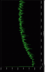
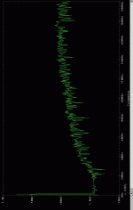
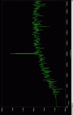
UcD (somebody could doubt?") based on [LM119_ST-> 74HC86->1N4148 (with res in parallel for dead time (10ns) adjusting)->74HC14->Ideal VSwitch Ron=.2ohm+MBR1045 as body diode.] with propagation delay about 120ns.
based on [LM119_ST-> 74HC86->1N4148 (with res in parallel for dead time (10ns) adjusting)->74HC14->Ideal VSwitch Ron=.2ohm+MBR1045 as body diode.] with propagation delay about 120ns.
Optimization criterion: min THD at 10khz@60khz_band for 1/1.4us idle switching.
Surprize number one:
Seems, the same named models isn't exactly matched for simulators. e.g., above mentioned res for dead time adjusting must be 1.4k for MC7 vs 5k for Pspice, the idle switching frequencys was difference (around 20%) too. Later i plan to use exact matched models (by copy/paste txt area).
Surprize number two:
The min THD at 10khz@60khz_band for 1/1.4us idle switching are comparable for a both simulators. (Please note, that's THD value found by me and i'm sure that it's rather not best of possible value, because i just a DIYer [hmm, sounds like my 2nd name].) When values of the feedback components (actually only two equal caps in the input filter, however difference isn't little -3.3n vs 9.1n) paste from MC7 to Pspice and vice versa, the THD figures is comparable again (.02%&.016%). MC7 give lower dependance THD from frequency, and i saw it in reality, unfortunately more then 24khz bandwidth invisible for me (no AP- no happy), "to be honest" this circuit version aren't checked so far. Some time ago Jan-Peter said that fully differential input is more preferable, so i've complete new PCB.. layout come quite ugly yet vs p2p, i need a time to do fixing some issues around stable oscillation (i miss on a hysteresis.
Surprize number three:
They behave differently, it's true..
MC7 really faster, 2 times at least, but i don't know why MC7 programmers didn't automatically zerocrossing detection for correct FFT, IMHO, it's a student task.
ok, MC or Pspice is not so matter for me vs real testing, i've not the tend to see in reality third kind of simulators. For my level of the practical class D implementation, MC is pretty useful.
Resume is coming soon.
all this aren't so much simple, Charles..
About analysed subject:
UcD (somebody could doubt?
based on [LM119_ST-> 74HC86->1N4148 (with res in parallel for dead time (10ns) adjusting)->74HC14->Ideal VSwitch Ron=.2ohm+MBR1045 as body diode.] with propagation delay about 120ns.Optimization criterion: min THD at 10khz@60khz_band for 1/1.4us idle switching.
Surprize number one:
Seems, the same named models isn't exactly matched for simulators. e.g., above mentioned res for dead time adjusting must be 1.4k for MC7 vs 5k for Pspice, the idle switching frequencys was difference (around 20%) too. Later i plan to use exact matched models (by copy/paste txt area).
Surprize number two:
The min THD at 10khz@60khz_band for 1/1.4us idle switching are comparable for a both simulators. (Please note, that's THD value found by me and i'm sure that it's rather not best of possible value, because i just a DIYer [hmm, sounds like my 2nd name].) When values of the feedback components (actually only two equal caps in the input filter, however difference isn't little -3.3n vs 9.1n) paste from MC7 to Pspice and vice versa, the THD figures is comparable again (.02%&.016%). MC7 give lower dependance THD from frequency, and i saw it in reality, unfortunately more then 24khz bandwidth invisible for me (no AP- no happy), "to be honest" this circuit version aren't checked so far. Some time ago Jan-Peter said that fully differential input is more preferable, so i've complete new PCB.. layout come quite ugly yet vs p2p, i need a time to do fixing some issues around stable oscillation (i miss on a hysteresis
.Surprize number three:
They behave differently, it's true..
MC7 really faster, 2 times at least, but i don't know why MC7 programmers didn't automatically zerocrossing detection for correct FFT, IMHO, it's a student task.
ok, MC or Pspice is not so matter for me vs real testing, i've not the tend to see in reality third kind of simulators
. For my level of the practical class D implementation, MC is pretty useful.Resume is coming soon.
Hi guys,
IVX, so you aren't able to see how close the simulators are to a real life implementation? That's too bad, do you just simulate until they are perfected and then build them? To they tend to work the first attempt?
Ok guys I got my gate drive wave forms looking much better, and consequently am only getting +-10 amps of cross conduction instead of the +-200 amps I experienced earlier.
Non the less, I find that the driver circuit lacks noise immunity, and would be difficult to optimise in order to maximize the noise immunity that it can have.
Therefore I've started with a new gate drive design which should keep dead time as minimal while eliminating any chances of cross conduction, while keeping part count about the same.
I also see no reason why this implementation wouldn't be a champ to simulate with so I am working on it, keep ya posted.
Regards,
Chris
How do you go about getting a db reading from uA? You're taking the current through the load?
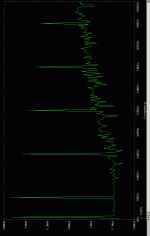
Yes I am measuring the current through the load. Simply out of lazyness. I'd have to scroll down a little more to find the voltage across the load resistor. Since the scale is logarithmic and the vertical lines are placed at powers of 10 they also indicate 20 dB increases.
Some more remarks to the amp. As already mentioned it is a hypothetical amp. It is capable of 1 Volt peak into 6 ohms. For this simulation it wouldn't matter whether the amp is capable to generate 1 Volt or a Kilovolt at it's output (a convenience one wouldn't have with a real-world amp unfortunately). But it is much more convenient to derive the parameters when everything is referenced to 1 Volt.
Feedback is a mixed solution before and after the output filter.
Regards
Charles
classd4sure,
<so you aren't able to see how close the simulators are to a real life implementation?> yeah, 1 week at least..
<To they tend to work the first attempt?> Usually... Why no? Actually, my day job require to be attentive(st), careful(st) and fast(st) every day (due to it i'm still alive. Some of the my skills (typical 2 minutes for replacing P-MQFP-44-2 only by Ersa-c25 iron) maybe better vs Bruno even!! (can i do dreaming?) ;-)
Charles,
how much at -3db THD, and whether it's available more details before patenting?
<so you aren't able to see how close the simulators are to a real life implementation?> yeah, 1 week at least..
<To they tend to work the first attempt?> Usually... Why no? Actually, my day job require to be attentive(st), careful(st) and fast(st) every day (due to it i'm still alive
. Some of the my skills (typical 2 minutes for replacing P-MQFP-44-2 only by Ersa-c25 iron) maybe better vs Bruno even!! (can i do dreaming?) ;-)Charles,
how much at -3db THD, and whether it's available more details before patenting?
IMD, when fed with 100 kHz and 101 kHz @ -12B each.
At the output they appear attenuated by 7 dB approx, due to the output filter.
IMD products below 20 kHz are attenuated by 85 dB approx (it is in fact more, if the attenuation of the "payload" at 100 kHz is taken into account).
I know that this would be a very severe test and not even HF hash from SACD and the like would amount to this.
OTOH it is never bad if a switching amp is as immune to HF hash as a good linear amp is, in order to nullify one of the the class-d oponents' arguments.
These are just simulations of course and one would have to build the thingie in order to know how it sounds. Fine-tuning of a delta-sigma modulator might be quite a task due to the amount of parameters involved.
I would like to keep the basic modulator topology secret at the moment. But I will soon publish the way I "implemented" the feedback-takeoff since this can be used for many different class-d topologies.
Regards
Charles
Attachments
Within post #52 I wrote:
It is of course NOT THD+N that has increased but the Signal/THD+N RATIO.
When we're at it. I also simulated 1 kHz sine-wave and 10 kHz rectangular. Both 12 dB below clipping.
The picture below shows the output signal (again current through load out of lazyness).
The noise-like switching residual, typical for sigma-delta modulation, can be seen riding on the top and bottom.
Regards
Charles
As expected, the THD+N has increased.
It is of course NOT THD+N that has increased but the Signal/THD+N RATIO.
When we're at it. I also simulated 1 kHz sine-wave and 10 kHz rectangular. Both 12 dB below clipping.
The picture below shows the output signal (again current through load out of lazyness).
The noise-like switching residual, typical for sigma-delta modulation, can be seen riding on the top and bottom.
Regards
Charles
Attachments
Hi,
@IVX
The reason I asked that, I'm aware of certain difficulties with the class D topology.....high speed switching.........etc
Do you attempt to model any non linearities ....trace inductances.....etc... How important are they really?? You dont' require that level of a circuit just to simulate the theory behind it, but to then take that exactly straight to pcb...that could be another story.
Based on your experience, would you worry about such additions to the simulation model, before ever trying to actually build it, or are such things best left for real world tweaking under a scope?
Excellent simulator comparison work! From reading EDAcafe spice handbook section they often do up the same circuit in a few simulators, Ispice, Pspice, and MC. They tell you what difficulties they had with one over the other, the fix required, run time for all three..
Ispice seems fastest overall, but the results from all three are always excellent with their breadboarded circuit.
@phase_accurate,
I would enjoy reading about your implementation of a dual feedback loop, anything like ICEpower?
I like seeing how you play with the graphs to test your circuit out, shows some nice advantages to simulations that would be alot more of a pain to do in reality, to achieve meaningful results. As per the topic ....and since we took off into simulator land, perhaps you'd be so kind as to recommend a small number of "basic, must do" tests such as these, which would have meaningful results for class D implementations, and aren't the usual bode plots, also stating expected results/what to look for, if not already obvious.
This would be for the sole purpose of establishing a class d standard of basic tests, specifically for simulators, which we can all use to compare results against others circuits.
Any tests specific to circuit implementation should of course be omitted.
My update:
I've managed to test a few quick layouts of my new driver, got one partially working. Upon more research, I've discovered I need to dwelve deeper into the land of spice in order to produce a better modeled circuit, which should solve all problems I'm currently experiencing with it.
I expect the research required will take a fair bit of time, in reality this could be changed in a matter of minutes, while I'll be spending hours, if not day's, learning exactly how to model my part realistically. Simulators can save some time, they can also slow things right down, all part of the learning curve.
Regards,
Chris
To they tend to work the first attempt?> Usually... Why no?
@IVX
The reason I asked that, I'm aware of certain difficulties with the class D topology.....high speed switching.........etc
Do you attempt to model any non linearities ....trace inductances.....etc... How important are they really?? You dont' require that level of a circuit just to simulate the theory behind it, but to then take that exactly straight to pcb...that could be another story.
Based on your experience, would you worry about such additions to the simulation model, before ever trying to actually build it, or are such things best left for real world tweaking under a scope?
Excellent simulator comparison work! From reading EDAcafe spice handbook section they often do up the same circuit in a few simulators, Ispice, Pspice, and MC. They tell you what difficulties they had with one over the other, the fix required, run time for all three..
Ispice seems fastest overall, but the results from all three are always excellent with their breadboarded circuit.
@phase_accurate,
I would enjoy reading about your implementation of a dual feedback loop, anything like ICEpower?
I like seeing how you play with the graphs to test your circuit out, shows some nice advantages to simulations that would be alot more of a pain to do in reality, to achieve meaningful results. As per the topic ....and since we took off into simulator land, perhaps you'd be so kind as to recommend a small number of "basic, must do" tests such as these, which would have meaningful results for class D implementations, and aren't the usual bode plots, also stating expected results/what to look for, if not already obvious.
This would be for the sole purpose of establishing a class d standard of basic tests, specifically for simulators, which we can all use to compare results against others circuits.
Any tests specific to circuit implementation should of course be omitted.
My update:
I've managed to test a few quick layouts of my new driver, got one partially working. Upon more research, I've discovered I need to dwelve deeper into the land of spice in order to produce a better modeled circuit, which should solve all problems I'm currently experiencing with it.
I expect the research required will take a fair bit of time, in reality this could be changed in a matter of minutes, while I'll be spending hours, if not day's, learning exactly how to model my part realistically. Simulators can save some time, they can also slow things right down, all part of the learning curve.
Regards,
Chris
I would enjoy reading about your implementation of a dual feedback loop, anything like ICEpower?
It is much simpler and it aids the feedback takeoff after the output filter. Many people have difficulties taking feedback from the filter due to issues with phase-margin. So the circuit would be most useful for carrier-based circuits and sigma-delta topologies.
When you implement a self-oscillating circuit like UCD you don't usually bother with phase-shift, rather the contrary is the case since it helps you getting the thing oscillating !
I will put together some basics around feedback topology for carrier-based class-d amps and put them on this forum. But it will take some time.
Regards
Charles
Hi,
HAH, I was just doing some reading on control theory........WHEW, and ya can't even get the goods online. I'd like to attain a much more intuitive level of understanding, then I'd be dangerous.
At this point, honestly, I've no idea how or why carrier based/non carrier based feedback topologies should differ, an area of much confusion and very little information, Sir, you serve this forum well. Take your time with it, we can wait for the good stuff.
We seriously need a dedicated class d forum here before this all starts to get lost amongst the archives of Cdom compensation.
Regards,
Chris
HAH, I was just doing some reading on control theory........WHEW, and ya can't even get the goods online. I'd like to attain a much more intuitive level of understanding, then I'd be dangerous.
I will put together some basics around feedback topology for carrier-based class-d amps and put them on this forum. But it will take some time.
At this point, honestly, I've no idea how or why carrier based/non carrier based feedback topologies should differ, an area of much confusion and very little information, Sir, you serve this forum well. Take your time with it, we can wait for the good stuff.
We seriously need a dedicated class d forum here before this all starts to get lost amongst the archives of Cdom compensation.
Regards,
Chris
Charles,
your plots (noiseshaper like) show gave reason to suspect that your amp have second feedback loop above modulator? Of course listening is needed. Regarding UcD+2nd_loop, i left my attempt at same day when started, because sound degradation was more than expected. Probably UcD (any amp too?) simplicity is more needed for listener, then for DIYer even? (Bruno, Jan-Peter, i'm right or a not? BTW, what about yours listening with optimal 2nd loop?)
Chris,
i use only simplified models of amps, without mosfet even to avoiding convergence troubles to keep time for real experiments. (i would do more of real experiments and less simulations if i've more time). But my experience is really poor.
No listening results yet with the higher order loop UcD's. Once JP has time again I'll be compelled to make some myself too
The key issue is obtaining reliable overload stability (same problem as deltasigma at overload)
I suspect that a deltasigma amp can sound OK but you really need to go to 5th order or so.
The key issue is obtaining reliable overload stability (same problem as deltasigma at overload)
I suspect that a deltasigma amp can sound OK but you really need to go to 5th order or so.
- Status
- This old topic is closed. If you want to reopen this topic, contact a moderator using the "Report Post" button.
- Home
- Amplifiers
- Class D
- Distorsions in class D